The undercutting process of thermal SiO2 microcantilevers with differentorientations on (100) Si wafer was studied. The silicon substrate was removed byanisotropic chemical etching with a 25 wt. % aqueous solution of TMAH or a 30 wt. %aqueous KOH solution at 80 °C. It was found that 〈110〉 oriented cantilevers wereundercutting frontally along the length and 〈100〉 oriented cantilevers experienceundercutting along the width of the cantilever, which is a less time consuming process. The studies showed that the 〈100〉 orientation of SiO2 microbridges enablestheirs fabrication on a (100) oriented Si substrate.
Since its discovery in the middle of the 1960s, anisotropic wet chemical etching1 of single crystal silicon (sc Si) has been widely used in the semiconductorindustry. Nowadays this technique is applied in the fabrication of different typesof sensors and actuators and optical components in micro-electro-mechanical-system (MEMS) technologies.
Microcantilevers and microbridges are one of the major diagnostic structuresnot only in a variety of sensors,3 but also for measuring mechanical (e.g. residualstress and Young’s modules)4 or thermal (e.g. thermal expansion coefficients)5properties of thin films used in MEMS technologies.
This paper describes the experimental results used to investigate the correlation between the orientation of the microcantilevers and microbridges after anisotropic wet etching of silicon substrates. In the fabrication of SiO2 microcantilevers or microbridges, anisotropic wet etching of Si substrate beneath the SiO2film creates free standing structures. Silicon dioxide is relatively insoluble in aqueous alkaline solutions of TMAH (tetramethylammonium hydroxide) or KOH whichare used for anisotropic etching.2 SiO2 thin films are transparent which enablesthe observation of the Si undercut processes during etching. Conclusions aboutthe anisotropic etching of sc Si substrates could be useful in etching microcantilevers made from opaque materials insoluble in these solutions. Also, many SiO2-based microcantilever systems are successfully designed and fabricated for variousMEMS applications.6,7 Hence, the main aim of this work was to establish the conditions for Si substrate undercutting during the course of etching and find the optimal orientation of the released microcantilevers and microbridges.
The SiO2 microcantilevers used for these experiments had been fabricated on n-type (boron-doped) sc Si wafers with the (100) orientation. The Si wafers were mirror polished and has resistivityvalues between 5 and 3 Ω cm. Approximately 1 µm thermal oxide was grown on the Si substrate inoxygen ambient saturated with H2O vapor. The temperature for the silicon oxide growth was 1115 °C.Designed structures were patterned using a standard photolithographic technique8 and openings inthe SiO2 were etched using a buffer oxide etch. The cantilevers patterns were aligned to the primewafer flat on the (100) Si substrate, i.e., along the 〈110〉 direction. Two types of cantilevers and microbridges orientations were investigated: one parallel to the prime flat or aligned to the 〈110〉 direction and the other was oriented to the 〈100〉 direction, which is 45° from the prime wafer flat. Thedimensions of the designed cantilevers and microbridges were 25, 50 or 100 µm in width and 100,200, 300 or 500 µm in length.
The etching process was carried out using two alkaline solutions which are the most frequenttly used in MEMS processing, namely: a 25 wt. % aqueous TMAH solution or a 30 wt. % aqueousKOH solution. The solutions are held in a thermostated Pyrex glass vessel at the etching temperature of 80 °C (temperature stabilization ±0.5 °C) for both solutions. The vessel was sealed with a screwon lid which included a tap water cooled condenser, to minimize evaporation during the etching.During the etching, the wafer was held in a Teflon holder in the horizontal position above a magnetic stirrer bar. The solution was electromagnetically stirred at 700 rpm. A detailed description ofthe apparatus is given in the literature.
After the etching process, the etched wafers were removed from the solution and thoroughlyrinsed with deionized water without the application of any procedure10 for the prevention of cracking or stiction of the released microcantilevers. In future work with the aim of fabricating microcantilevers for specific application, drying and stiction problems should be resolved because theyare directly connected with yield of fabricated devices.

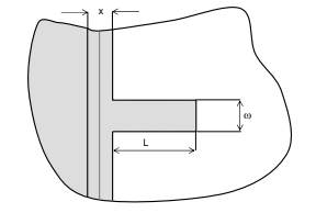
Fig1
By measuring the etching depth in the 〈100〉 direction for a given etching time, it is possible to determine the etching rate (Eq. (1)) of the (100) planes inboth solutions. Etching rates are 0.44 µm min−1 for the 25 wt. % aqueous TMAHsolution at 80 °C and 1.30 µm min−1 for the 30 wt. % aqueous KOH solution at80 °C. The etching rate of the sloped {111} planes were determined in both solutions using Eq. (3), knowing the slope angle (θ = 54.7°) and measuring x for agiven etching time. The determined etching rates of the {111} planes are 2.2×10⁻²and 5.0×10⁻³ µm min−1 for the TMAH and KOH solution, respectively.