ABSTRACT
MOS High Electron Mobility Transistors (MOS-HEMTs) may suffer from VTH instability and hysteresis reducing device performances. Post-Deposition Anneal (PDA) of the Atomic-Layer Deposited (ALD) dielectric has the potential to increase MOS-HEMT performances but needs to be compatible with the actual integration (at CEA Leti: fully recessed Gate First MOS-channel HEMT process flow). In this work, the impact of different PDA temperatures on flat-band voltage (VFB) and its hysteresis (ΔVFB) for Al2O3 deposited on etched GaN substrates is investigated using MOS capacitors (MOSCAPs). Material properties are analyzed by Hard X-Ray Photoelectron Spectroscopy (HAXPES), Fourier Transform Infrared Spectroscopy (FTIR) and Time-of-Flight Secondary Ion Mass Spectrometry (ToF-SIMS) analyses. With increasing PDA temperature up to 500◦C: (i) ΔVFB decreases and is explained by the reduction of Ga-O bonds at Al2O3/GaN interface and O-H groups in Al2O3 (ii) VFB decreases and could be explained by the reduction of fluorine impurity concentration in Al2O3. For 600◦C PDA, Grazing Incidence X-Ray Diffraction (GIXRD) analysis shows a small crystallized κ-Al2O3 signal on etched GaN contrary to the as-grown GaN. The onset of this crystallization could explain the degradation in breakdown field for PDA above 500◦C observed on MOSCAPs after the Gate-First process flow overall thermal budget. Therefore, the optimized PDA temperature suggested for a fully recessed Gate First MOS-channel HEMT is 500◦C.
1. Introduction
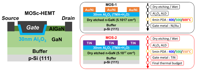
Due to their two-dimensional electron gas (2DEG) obtained from AlGaN/GaN heterojunction, GaN based high electron mobility transistors (HEMTs) are interesting for the field of power electronics where higher switching frequency and reduced on-state-resistance (Ron) are required. HEMTs are normally-on devices with a negative threshold voltage (VTH<0). However, for safety issues and simplified driver systems design, HEMTs with a positive threshold voltage addressed as “normally-off” are highly demanded. One approach is the partial recess of the AlGaN barrier, increasing VTH by reducing the 2DEG, but with the drawback of having a VTH sensible to small variations in the recess depth. To overcome this issue, the MOS-channel HEMT (MOSc-HEMT) with its fully recessed AlGaN barrier and MOS gate (Fig. 1) totally depletes the 2DEG assuring a positive VTH, and reduces the gate current leakage . Still, its VTH depends on the gate dielectric Al2O3/etched GaN interface properties . Post-Deposition Anneal (PDA) of Al2O3/GaN has been reported to increase the threshold voltage and reduce its hysteresis (ΔVTH) . Except for Kim et al., most of these reports are for Al2O3 deposited either on as-grown or etched GaN substrates using a Gate-Last process flow in which the source and the drain fabrication is carried before the gate fabrication. Since our MOSc-HEMT process flow is Gate-First with a final thermal budget including ohmic contact annealing , the impact of Al2O3 PDA deposited on etched GaN for the Gate-First process flow is investigated with electrical and chemical characterizations.

Fig. 1. On the left, the schematic representation of a MOSc-HEMT. On the right, the schematic representation and process flows for MOS-1 and MOS-2.
2. Materials and methods
In order to reproduce the MOSc-HEMT gate processing, 30nm of Al2O3 was deposited by Atomic Layer Deposition (ALD) at 300◦C using TMA and H2O precursors on dry etched nGaN/Si wafers. The 200mm nGaN/Si wafers were grown using Metal Organic Chemical Vapor Deposition (MOCVD) on Si substrates, with an GaN n-type doping of 5.1017 cm− 3 . The dry etching was performed using Inductively Coupled Plasma Reactive Ion Etching (ICP-RIE) with chlorine-based chemistry. A wet cleaning containing HF was carried out before Al2O3 deposition. Since minor consensus is found for PDA’s duration, with duration ranging from 30s to 90min , a low PDA’s duration is performed. Hence, after ALD, PDA was performed under N2 1) for 4 min at 400, 500, and 600◦C on 1.5 cm × 1.5 cm samples or 2) for 5 min at 400, 500, and 550◦C on 200mm wafers. MOSCAPs test structures were then fabricated: 1) on the 1.5 cm × 1.5 cm samples with Au/Ni metal contacts deposited by e-beam evaporation (MOS-1) and 2) on the 200 mm wafers with TiN metal contacts deposited by Physical Vapor Deposition (MOS-2). The MOS-2 devices were annealed after metal deposition to simulate the Gate-First thermal budget including a rapid thermal annealing which was in the temperature range of 400-650◦C. The process flows for the two devices are summarized in Fig. 1.
For physical and chemical characterizations, specific Al2O3/GaN samples were prepared with the same processing conditions but with only 15nm of Al2O3. The PDA conditions were the same as for MOS-1 devices. Hard X-Ray Photoelectron Spectroscopy (HAXPES), Time-ofFlight Secondary Ion Mass Spectrometry (ToF-SIMS) and Grazing Incidence X-Ray Diffraction (GIXRD) were performed on these dedicated samples. HAXPES analyses were conducted on a PHI Quantes, equipped with both monochromatic Al Kα (hν=1486.7 eV) and Cr Kα (hν=5414.7eV) X-Ray sources, the last one allowing the analysis of buried interfaces. Since the C1s intensity is strongly reduced with a Cr Kα source, the binding energy was calibrated with the O1s peak (531.2eV), as measured using the Al Kα source and referenced to the C1s peak (284.8eV). The photoelectron take-off angles were set at 45◦ (Ga2p3/2) and 90◦ (O1s) respectively, yielding integrated sampling depths of approximately 16.6 and 24 nm with the Cr Kα source. As seen in Fig. 2a, three contributions for Ga2p3/2 were used: Ga-N (~1117.8eV), Ga-O (~1118.4eV) and Ga-Ga (~1116.5eV). In order to have a comparable analysis, the energy shifts of Ga-O and Ga-Ga with respect to Ga-N were fixed at 0.7eV and -1.3eV respectively. GaN oxidation at the interface was analyzed with the Ga-O area percentage in Ga2p3/2 peak. Similarly, O1s peaks were analyzed using O-Al (~531eV) and O-H (~532.2eV) contributions, the energy shift between O-H and O-Al being fixed to 1.2eV . The O1s spectrum with the associated peak fitting is shown in Fig. 2b. As for gallium oxide, the presence of O-H groups was deduced from the area of O-H bonds in O1s peak.

Fig. 2. a) Ga2p3/2 spectrum from the reference with a take-off angle of 45◦; b) O1s spectrum from the reference with a take-off angle of 90◦.
3. Results and discussion
PDA without final thermal budget
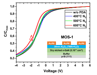
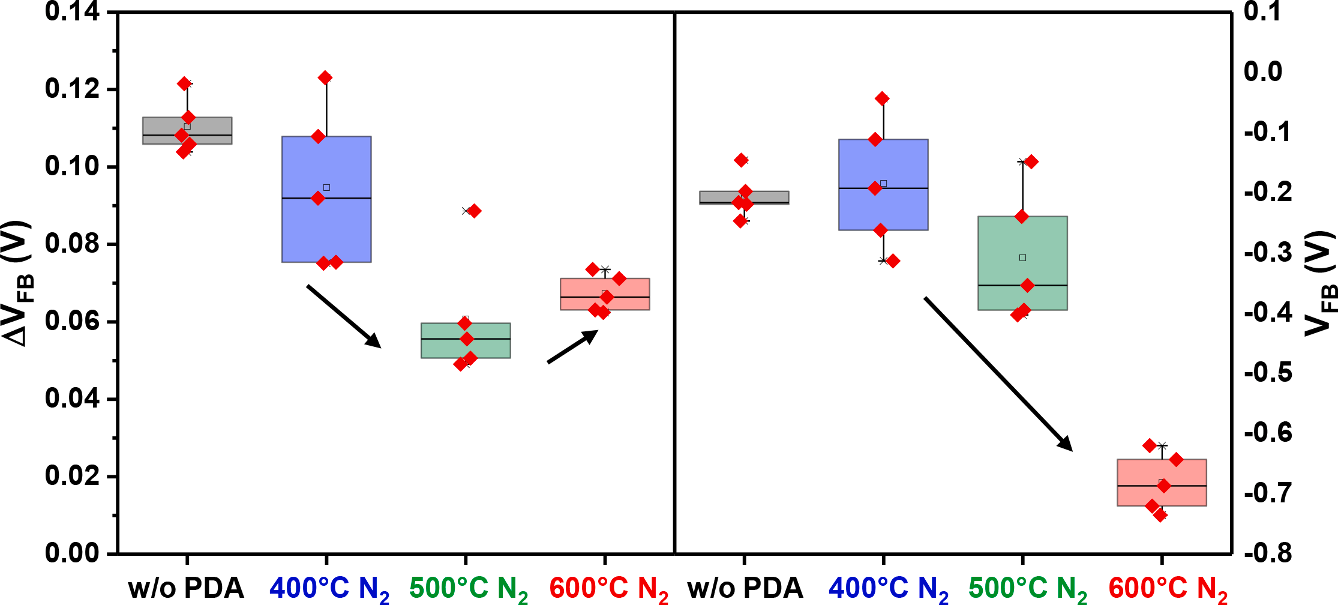
The C-V measurements for MOS-1 devices are reported in Fig. 3, with ΔVFB and VFB being extracted and shown in Fig. 4. ΔVFB is reduced with increasing PDA temperature until a minimum at 500◦C, reducing from 108mV to 56mV between the reference and the PDA at 500◦C. The reduction of ΔVFB with PDA temperature was similarly observed in previous reports . However, for a PDA over 500◦C, an increase of ΔVFB is observed.

Fig. 3. Normalized C-V characteristics at 1 kHz for MOS-1 devices (median of five measurements).

Fig. 4. ΔVFB and VFB for MOS-1 devices extracted from C-V measurements.
4. Conclusion
The impact of PDA for Al2O3 on etched GaN substrates for Gate-First MOSc-HEMTs process flow was investigated with both electrical and chemical characterizations. In the case of PDA below 500◦C without the final thermal budget, the beneficial reduction of hysteresis is observed, correlated to the reduction of GaOX at the Al2O3/GaN interface and OH groups in the alumina. A small reduction of VFB following the trend of fluorine reduction in Al2O3 is also observed. However, for a PDA above 500◦C, the hysteresis increases likewise linked to the increase of GaOX.
With the device final thermal budget, the PDA’s effect on VFB is reduced. However, the degradation of hysteresis is equally observed for a PDA over 500◦C. Furthermore, a degradation of breakdown field is observed and is explained by the beginning of Al2O3 crystallization appearing only on etched GaN substrates.
Therefore, the overall thermal budget and the GaN processing prior to Al2O3 deposition, both influence the impact of PDA; these parameters should be taken into account when optimizing the PDA for the Gate-First approach. The best PDA conditions so far for our MOSc-HEMT architecture seem to be 500◦C.
下一篇: V 型槽硅基板上 GaP 的聚结