ABSTRACT:
Here, we study the morphology and dislocation dynamics of metalorganic vapor phase epitaxy (MOVPE)-grown GaP on a V-groove Si substrate. We show that Si from the substrate stabilizes the (0 0 1) GaP facet, which is critical for achieving coalescence. The SiNx caps covering the (0 0 1) tops of the V-grooves must be sufficiently small for the 3 × 1 GaP surface reconstruction caused by Si to continue to influence the GaP coalescence while the V-grooved sidewalls are covered. If the SiNx caps are too large, (1 1 1) diamond faceting develops in the GaP, and coalescence does not occur. On samples where coalescence is successful, we measure a root-mean-square roughness of 0.2 nm and a threading dislocation density of 5 × 107 cm−2 . Dislocation glide was found to begin during coalescence through transmission electron microscopy. With further TDD reduction, these GaP on V-groove templates will be suitable for III-V optoelectronic device growth.

The direct growth of high-quality III-V semiconductors on Si substrates for optoelectronic devices has been a key research goal for decades. Recently, advances in the control of crystalline defects in the epitaxial III-V layers has enabled rapid performance increases for III-V-on-Si solar cells and lasers. V-groove Si, a type of selective area growth (a strategy used in many epitaxial systems) where a substrate uses selective etching of nanopatterns to produce {1 1 1}- faceted trenches on a (0 0 1)-oriented Si wafer, is one of the technologies that has enabled this progress. The {1 1 1}- faceted surface of these templates stops the formation of antiphase domains (APDs), which historically have been a persistent problem for III-V-on-Si growth. V-grooves have been used for the direct growth of GaAs,InP, GaSb, and GaP on Si for laser and solar cell applications via metalorganic vapor phase epitaxy (MOVPE). We previously studied the nucleation of GaP on V-groove Si and identified suitable high-temperature growth conditions for GaP nucleation.In this work, we explore the coalescence of MOVPE-grown GaP on V-groove Si to establish a suitable III V-on-Si template for optoelectronic device growth.
For applications requiring continuous, large-area III-V thin films, V-groove Si adds a degree of complexity that is not present for growth on planar substrates or selective area growth not requiring thin films. Namely, material nucleated in neighboring grooves must coalesce to form a thin film. As opposed to conventional thin-film growth on planar substrates, conformal growth on the V-groove substrate is not always desired. For films grown by MOVPE, lateral growth is typically encouraged with a high V/III ratio to promote coalescence when growing over nanopatterns. Additionally, the dislocation dynamics differs between a V-groove system and planar substrates. The coalescence of relaxed, latticemismatched material can drive the formation of grown-in, sessile threading dislocations. Additionally, the shape of the V-grooves changes the strain profile in the III-V material and thus the driving force for dislocation glide.
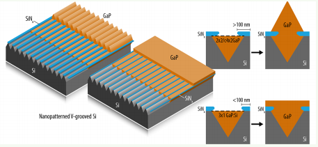
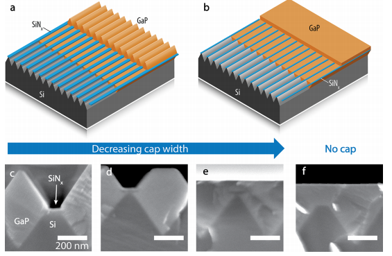
The scanning electron microscopy (SEM) cross-sectional images in Figure 1 show a transition from (1 1 1)-faceted GaP growth41 to (0 0 1)-faceted GaP coalescence as the SiNx caps decrease in width. We observe that for caps less than 100 nm wide or for samples with no caps, the GaP coalesces into a thin film. For samples with a wider SiNx cap, the GaP develops a diamond-like morphology with {1 1 1} faceting after it fills the grooves and does not coalesce. We always observed (0 0 1)- faceted growth in the V-groove trenches, regardless of cap width. We investigated a number of additional factors as possible variables controlling morphological evolution; we observed that the reactor history, the magnitude of sample offcut, direction relative to the V-grooves, and the details of the wet chemical and AsH3 pretreatments had no effect on the morphological evolution of GaP as it grew over the V-grooves. The role of the cap thickness was not investigated here but is expected to follow a trend with some maximum thickness beyond which the GaP does not coalesce.

Figure 1. (a,b) Schematics of GaP on V-groove Si with a (1 1 1) diamond morphology (a) and a coalesced (0 0 1) morphology (b). (c−f) SEM cross-sectional images of GaP grown on Si, with varying SiNx cap widths on V-grooves with a 500 nm spatial period. Diamond morphologies are produced for larger cap widths (a,b), whereas flat morphologies are produced when the SiNx cap is under 100 nm wide (c) or not present (d). All samples were grown together in the same run (WB989) at Tg = 800 °C and V/III = 5000.
One factor that changes between growth within the vgrooves and growth after filling is the presence of the exposed Si substrate. The change in GaP faceting upon the complete filling of the V-grooves points to a change in the surface energy of the (0 0 1) GaP surface at that point in the growth. At the high temperature at which the GaP is grown, it is likely that the Si from the exposed sidewalls is transported to the GaP surface via vapor phase transport and/or surface diffusion. Once the Si sidewalls are covered with GaP, there is no longer a source of surface Si present. As Si has been observed to influence the surface reconstruction of GaP,46 we hypothesize that the mobile Si supplied from the V-groove sidewalls stabilizes the (0 0 1) facet.
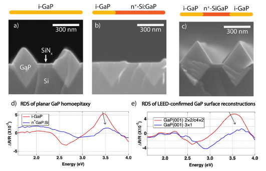
To more directly study the effect of Si on the GaP surface, we carried out a series of three experiments using Si2H6 flow during GaP growth to mimic the effect of Si transport onto the GaP surface from the V-groove sidewalls. The SiNx caps for these samples were 200 nm wide, ensuring that growth would be expected to have the diamond morphology at our standard growth conditions. All growth began with unintentionally doped GaP nucleation and growth in order to avoid influencing the nucleation process. After 12 min, the Vgrooves were about 1 /2 -filled with GaP, with exposed Si sidewalls remaining above the (0 0 1) GaP growth front (Figure S1a). After 30 min of growth, the V-grooves were completely filled (but not overgrown) with GaP still with an (0 0 1) surface (Figure S2b). For sample a, unintentionally doped GaP was grown for the entire 42 min (Figure 2a). For sample b (Figure 2b), unintentionally doped GaP was grown for 12 min, followed by GaP:Si under Si2H6 for 30 min to provide excess Si even after the sidewalls were covered. For sample c, unintentionally doped GaP was grown for 12 min, followed by GaP:Si under Si2H6 for 20 min, followed by unintentionally doped GaP for the final 10 min to show the morphology that forms without excess Si present. All three of these samples were grown for the same amount of time, with the same Ga flow throughout, at Tg = 800 °C and V/III = 5000. The 42 min of GaP growth used here provides sufficient time for the GaP to coalesce for samples with narrow caps.
SEM cross-sectional imaging (Figure 2) shows that the control sample (a) has the expected diamond morphology. The sample exposed to Si doping throughout the later portion of growth (b) did not coalesce into a thin film nor did it develop diamond faceting. This sample retained its (0 0 1) GaP faceting, with growth filling the grooves and then stopping. Finally, for the sample where Si doping was turned on and off again (c), the growth developed a diamond morphology. These results suggest, as hypothesized, that (1) Si stabilizes the (0 0 1) GaP facet at the growth conditions used in this work and (2) this effect can be reversed by removing the Si source. Intermediate growth steps after 12 and 32 min without any Si2H6 flowing are shown in the Supporting Information (S1).

Figure 2. (a−c) SEM cross-sectional images of GaP on V-groove Si comparing the impact of adding external Si dopants. All samples were grown under the same V/III ratio and temperature for the same length of growth time (V/III = 5000, Tg = 800 °C, time = 42 min). The bars above the images visually represent the flow of Si over the course of growth. Sample (a) was grown without Si2H6 (WC206); sample (b) had Si2H6 at the end of growth (WC150); and sample (c) had the Si source flowing for part of the growth (WC174). These three samples suggest that Si on the GaP growth surface suppresses the formation of {1 1 1} GaP facets. (d) shows RDS measured on homoepitaxial GaP wafers using the same growth conditions as for V-groove growth (WC323). (e) shows the RDS of a standard 2 × 2/c4 × 2 and a Si-contaminated 3 × 1 (0 0 1) GaP surface reconstruction from a previous study,46 where the surface reconstructions were confirmed with LEED (PC178).
Previous work has shown that the presence of some Group IV elements, such as Si and Ge, can produce a 3 × 1 surface reconstruction on III-Vs that results in a chemically inert (0 0 1) surface.46 Work on GaAs nanowires has also shown that dopant level Si can have a stabilizing effect on certain facets.47 In the current work, we observe a correlation between (0 0 1) GaP faceting and the supply of Si atoms to the GaP surface, and we hypothesize that these (0 0 1) GaP facets are similarly stabilized by Si atoms at the GaP surface. In this case, the Si could be supplied from the exposed Si surfaces until the grooves are filled with GaP. Our prior work was done on a growth reactor connected to an ultra-high-vacuum (UHV) chamber, enabling low-energy electron diffraction (LEED), scanning tunneing microscopy (STM), and Auger electron spectroscopy studies of the resulting 3 × 1 surface reconstruction.46 The current work was done in a standalone MOCVD chamber without these capabilities; however, both MOCVD chambers have in situ reflectance difference spectroscopy (RDS), providing a connection between current and prior work. A comparison was done using GaP (001) surfaces grown homoepitaxially on GaP substrates to avoid complications due to optical diffraction from the V-groove Si. GaP layers were grown both with and without Si doping, using the same Si flow as the experiments shown in Figure 2 at the optimized growth conditions described in the experimental section. Between layers, the wafer was cooled to 350 °C to measure RDS.
In conclusion, we have studied the morphology and dislocation dynamics of GaP as it coalesces into a thin film on V-groove Si. The width of the SiNx caps was found to be the determining factor in the final morphology of the films, with narrow caps (100 nm wide) resulting in thin-film coalescence. This effect was traced to the influence of Si on the surface reconstruction of the epitaxial GaP, changing it from a standard 2 × 2/c4 × 2 reconstruction to a 3 × 1 reconstruction that is thought to stabilize the (0 0 1) facet. Narrow SiNx caps likely allow the GaP to coalesce during a transient period where the V-groove Si sidewalls are covered, but the stabilizing influence of the Si remains on the (0 0 1) surface remains. Under conditions where coalescence occurs, AFM measurements showed a smooth surface with an Rq of 0.2 nm and visible atomic steps. ECCI showed that these films had a TDD of 5 × 107 cm−2 shortly after coalescence, a moderate value that is still too high for most optoelectronic devices; the development of further dislocation reduction strategies is ongoing. TEM combined with the observation of misfit dislocations spanning many grooves further suggests that lattice relaxation occurs via dislocation glide after coalescence. The GaP exceeded the experimental critical thickness for GaP grown on planar Si by approximately a factor of 3, perhaps due to differing strain fields from the V-grooves or changes to the kinetics of dislocation half loop nucleation from the atypical 3 × 1 surface reconstruction. For these films to be useful as optoelectronic device templates, future work must focus on decreasing the TDD.