Abstract:
Tunable semiconductor lasers have many important applications such as wavelength division multiplexing, light detection and ranging, and gas detection. The increased interest in silicon photonics has led to the rapid development of miniaturized on-chip tunable semiconductor lasers. However, silicon has poor light-emitting properties. Therefore, realizing high-performance tunable semiconductor lasers requires the integration of light sources with silicon. In this study, we review silicon-based light source integration methods and the development of siliconbased integrated tunable semiconductor lasers. Considering that narrow-linewidth performance greatly expands the applications of tunable semiconductor lasers, methods for reducing the linewidth of tunable lasers are summarized. Finally, the development trends and prospects for silicon-based integrated light sources and silicon-based integrated tunable lasers are analyzed and discussed.
1 Introduction
Tunable semiconductor lasers are indispensable and important components in many fields because they are small, light, integrable, and tunable to different lasing wavelengths, which makes such lasers suitable for a broad range of functions. For example, to satisfy high-speed and capacity communication requirements, dense wavelength division multiplexing (DWDM) is currently one of the most effective technologies in core and optical access networks . Tunable semiconductor lasers are vital light source devices in a DWDM system. For example, for a system with 96 channels and 50 GHz channel spacing, 38 nm wavelength tuning range is needed and the linewidth is in the order of 100 kHz . Due to the lack of frequency sources, the demand for tunable semiconductor lasers in ultra-DWDM systems will continue to increase. Tunable semiconductor lasers are also indispensable in the field of sensing, and light detection and ranging (LIDAR), especially optical phased array-based LIDAR, is currently being actively studied. Allsolid-state LIDAR requires a widely tunable semiconductor laser source that can be integrated into the same chip as an optical phased array, given that a wide tuning range ensures a large angle scan in the longitudinal direction. Tunable laser with output power of 20 mW, tuning range of 53 nm and linewidth of 100 kHz has been successful applied to an LIRDA system which achieves a scanning angle of 7◦. A 15◦ scanning angle requires a laser wavelength tuning range of 100 nm. As for a 20◦ scanning angle, the tuning range should be greater than 140 nm . Sweptsource optical coherence tomography uses tunable lasers as light sources because they exhibit ultra-high-speed scanning, non-invasive imaging, high-resolution, and real-time imaging. This makes them extremely valuable in medical clinical diagnosis applications. The tunable lasers in the system are required to tune fast to realize a high imaging speed. Devices achieve over 70 nm wavelength tuning at over 30 mW of output power and show a high imaging speed at 800 kHz A-scan rates. Moreover, tunable lasers can be used as a light source in gas detection to generate high-resolution characteristic absorption spectra of gases, thus improving the sensitivity of gas detection systems. In addition, tunable lasers have important applications in the fields of spectroscopy, terahertz communication, and optical clocks.
Like other optoelectronic devices, tunable lasers have known increasing development since their emergence. The production cost has been continuously reduced, which allowed large-scale production capacity. Integrated tunable semiconductor lasers have been receiving considerable attention as a research topic due to their small size, low cost, superior performance, and integrability. In addition, the rapid development of silicon optical technology provides new opportunities for tunable semiconductor lasers. Silicon, silicon dioxide, and silicon nitride are transparent in the 1300 and 1550 nm bands for standard communications and different material combinations can form high refractive index contrast to realize effective confinement of the optical mode field. This gives silicon-based optical waveguides superior performance to realize passive optical devices with different functions. In addition, they are compatible with the technologically mature complementary metal-oxide-semiconductor (CMOS) fabrication processes. This allows large-scale photonic device production at a low cost, providing a highly valued platform for optical interconnects. However, because silicon is an indirect-bandgap semiconductor, its luminescence performance is poor due to the simultaneous existence of free-carrier absorption, Auger recombination, and indirect recombination during the carrier transition process, resulting in very weak photon emission. The lack of an effective integrated light source has long restricted the development of silicon-based integrated photonic technology . In contrast to silicon, III–V materials have excellent light-emitting properties. Combining III–V materials with silicon to form a silicon-based integrated tunable laser has become an effective solution to the lack of light sources for silicon-based integration platforms. Considerable efforts have been made in this area in recent years.
2 Integration methods
An increasing number of researchers are focusing on integrating III–V gain media into silicon-based photonic platforms, owing to the excellent luminescent properties of III–V materials and the rapid development of silicon-based photonic technology. The main approaches can be divided into hybrid integration, heterogeneous integration, monolithic integration, and micro-transfer printing (μTP) . In this section, we will elaborate on these categories.

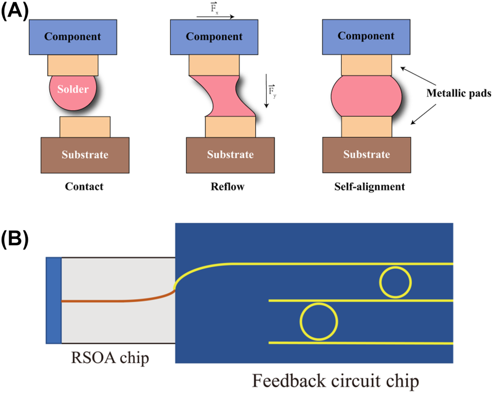
Figure 1: (A) Flip-chip self-alignment of the component and substrate during reflow. (B) In-plane butt-joint coupling method.
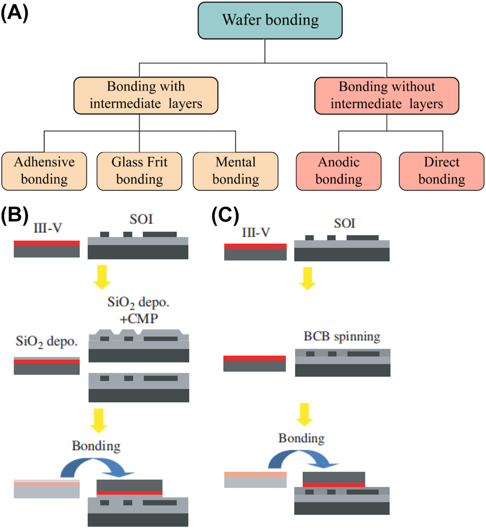
Direct bonding, first proposed by Lasky et al. in 1986, directly connects the surfaces of two mirror-polished semiconductor wafers by mechanical or electric field action without any intermediate layer. The two surfaces are in intimate contact through van der Waals forces or hydrogen bonding. However, this state is not automatically achievable because factors such as surface roughness, wafer unevenness, and the presence of microscopic particles prevent such close contact between the surfaces; thereby, after the two wafers are placed in contact, pressure is usually applied to the wafer center (or side) wherein the surfaces are in close contact, and localized bonding is achieved at the pressure point. Then, the wafer surfaces enter into close contact due to the attraction between the wafers, and the bonding wave spreads from the pressure point to the periphery of the wafer, achieving close contact in a few seconds. However, this adhesion is much weaker than covalent bonding, and subsequent high-temperature annealing is required. The annealing temperature is usually above 800 ◦C and can be reduced by plasma activation or other special wafer surface processing. A SiO2 direct bonding process is illustrated in Figure 2B .

Figure 2: (A) Wafer bonding technology classification. (B) SiO2 direct bonding. (C) Divinylsiloxane-bis-benzocyclobutene (DVS-BCB)
adhesive bonding.
Conclusions
In this study, we summarized and compared the research and development status of several different integration technologies, starting with silicon-based integration technology. Notably, hybrid and heterogeneous integration technologies have been widely studied and applied to silicon photonics platforms. Monolithic integration and μTP technologies are not yet mature; however, owing to their predicted large-scale integrability, low cost, and high integration density, among other excellent performance characteristics, they are expected to be the mainstream solution of integration technology in the future.
Tunable lasers have advanced over the decades and are currently evolving towards miniaturization, and integrated tunable lasers are the trend of the future. In this study, we investigated and summarized the recent developments of silicon-based tunable semiconductor lasers based on different integration methods. The linewidth has become one of the most important criteria for the performance of tunable semiconductor lasers. Narrow-linewidth wideband tunable semiconductor lasers have become the core light source for high-speed optical communication, coherent space laser communications, and coherent optical detection. In this study, starting with linewidth theory, we summarized the implementation methods and research progress of narrowlinewidth lasers. The material properties of silicon nitride make it a promising narrow-linewidth candidate that is likely to be used in future applications such as coherent optical receivers and transmitters, optical networks, and biosensing. Solving the problem of high refractive index mismatch between silicon nitride and III–V materials has become the key to realizing heterogeneous integrated narrow-linewidth tunable lasers on a silicon nitride platform.
In summary, silicon-based integrated tunable semiconductor lasers have become an essential light source in fields such as optical communications wavelength division multiplexing, LIDAR, and medical services. Further research is necessary to achieve better quality, higher yield, and costeffective integration methods. Wider and faster tuning, and narrower linewidth lasers are also promising avenues for future research.
上一篇: V 型槽硅基板上 GaP 的聚结
下一篇: 硅氧化铝表面钝化的激活:分离体和表面效应