ABSTRACT
Understanding surface passivation arising from aluminium oxide (Al2O3) films is of significant relevance for silicon-based solar cells and devices that require negligible surface recombination. This study aims to understand the competing bulk and surface lifetime effects which occur during the activation of atomic layer deposited Al2O3. We demonstrate that maximum passivation is achieved on n- and p-type silicon with activation at ~ 450 ◦C, irrespective of annealing ambient. Upon stripping the Al2O3 films and re-passivating the surface using a superacid-based technique, we find the bulk lifetime of float-zone and Czochralski silicon wafers degrade at annealing temperatures > 450 ◦C. By accounting for this bulk lifetime degradation, we demonstrate that the chemical passivation component associated with Al2O3 remains stable at activation temperatures of 450─500 ◦C, achieving an SRV of < 1 cm/s on n- and p-type silicon. In conjunction with the thermal stability, we show that films in the range of 3–30 nm maintain an SRV of < 1 cm/s when annealed at 450 ◦C. From atomic-level energy dispersive X-ray analysis, we demonstrate that, post deposition, the interface has a structure of Si/SiO2/Al2O3. After activation at > 300 ◦C, the interface becomes Si/SixAlyO2/Al2O3 due to diffusion of aluminium into the thin silicon oxide layer.
1. Introduction
Silicon photovoltaics account for > 95 % of the PV market, and this dominance is predicted to remain unchanged for the foreseeable future. With the mainstream PV technology being the passivated emitter and rear cell (PERC) architecture, mitigation of surface recombination through state-of-the-art passivation layers on the front and rear of the solar cell has become ever more important. In particular, the reemergence of aluminium oxide (Al2O3) in 2006 has enabled high levels of surface passivation to be achieved on the rear side of PERC solar cells (on a p-type substrate), which can be attributed to the high levels of negative charge and good chemical passivation properties of the film. Furthermore, with the recent introduction of passivating contact structures (e.g. TOPCon), Al2O3 passivation is now being utilised on the front surface of TOPCon solar cells which use n-type substrates. As such, Al2O3 is playing an ever-increasing role in mitigating surface recombination on either the front or rear surface, thereby demonstrating its significance in the development of highly efficient solar cells.
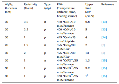
There remains some uncertainty in how one can maximise the highest level of surface passivation on silicon. Often, the level of surface passivation is quantified based on the effective lifetime level achieved, which is subsequently converted into a surface recombination velocity (SRV) or surface saturation current density (J0s). However, in doing so, the underlying bulk silicon material is assumed to be thermally stable at post-deposition annealing temperatures of < 500 ◦C. If this assumption is incorrect there can be substantial variability in the extracted values and thus any conclusions drawn from them. It has recently been shown that the bulk lifetime (τbulk) of float-zone (FZ) silicon is thermally unstable at temperatures between 400─800 ◦C, whereby τbulk has been shown to decrease by up to two orders of magnitude in some cases, independent of FZ silicon manufacturer. High temperature (>1000 ◦C) thermal treatments in an oxygen ambient have been shown to annihilate the point defects responsible for this instability in the bulk lifetime, however such processes are not readily available to all research groups, and thus are often omitted in sample processing. Czochralski (Cz) silicon wafers can offer greater thermal stability, as they do not possess the same point defects created in FZ silicon, however the bulk lifetime in ‘as-received’ wafers can degrade/improve via other mechanisms, such as oxygen-related defects (thermal donors, oxygen precipitation) and metal impurities. No silicon material can offer complete thermal stability of the bulk lifetime, and this could partly explain the variability in the passivation results reported in the literature. Setting aside material quality, and assuming similar deposition conditions, the main parameters that control Al2O3 surface passivation are found in the post deposition annealing conditions, as identified in Table 1. For the examples listed in Table 1, all studies have used FZ silicon as their base material without considering thermal degradation (or improvement), and each study used different post-deposition annealing conditions to achieve maximum surface passivation.

Table 1 A summary of ALD Al2O3 passivation on FZ silicon in key publications. All reported values are for films deposited at ~ 200 ◦C using an O2 plasma as the coreactant and trimethylaluminium as the precursor with the post deposition annealing (PDA) conditions as stated. Upper limit SRVs are for an injection level of 1015 cm− 3 .
2. Experimental methods
Silicon samples were prepared by first immersing them in a 2 % hydrofluoric acid (HF) solution to remove any native oxide present. The samples were then immersed in a standard clean 1 (SC 1) solution consisting of H2O, H2O2 (30 %) and NH4OH (30 %) (5:1:1) at ~ 75 ◦C for 10 min. Following the SC 1 clean, the samples were once again immersed in a fresh 2 % HF solution to remove the chemical oxide formed during the cleaning process, and subsequently immersed in a 25 % TMAH etching solution at ~ 80 ◦C for 10 min. Thereafter, the samples were immersed in fresh 2 % HF solution and then immersed in a standard clean 2 (SC 2) solution consisting of H2O, H2O2 (30 %) and HCl (37 %) (5:1:1) at ~ 75 ◦C for 10 min. To complete the surface pre-treatment, samples were immersed (individually) in a 2 % HF-HCl solution for ~ 5 s and pulled dry from the HF-HCl solution to give a hydrogen terminated surface [17]. At this point the samples were not rinsed in deionized (DI) water.
Immediately following the wet chemical cleaning process, the samples were transferred to the load lock of a Veeco Fiji G2 system which was then subsequently evacuated to mitigate any unintentional oxide formation. 5–250 cycles of Al2O3 (0.7–35 nm assuming a growth rate of 0.13 nm ) were deposited by ALD at 200 ◦C using an O2 plasma source and trimethylaluminum precursor. The deposition was performed on both sides of the samples to achieve symmetrical structures. Following the Al2O3 depositions, the samples were annealed in a quartz tube furnace for 30 min in air at a specified annealing temperature. In some cases, silicon samples were annealed in a Surface Science Integration Solaris 100 rapid thermal processor (RTP) for 30 min at a specified annealing temperature and ambient (N2, forming gas or N2O). For this study, a 30 min anneal was chosen to ensure enough time was allowed to achieve maximum passivation, especially for lower annealing temperatures.
3. Results and discussion
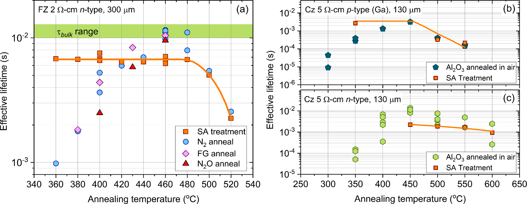
Fig. 1 (a) plots the effective lifetime (at an excess carrier density, Δn = 1015 cm− 3 ) of ALD Al2O3 coated (~20 nm) FZ 2 Ω-cm n-type silicon materials after annealing at temperatures between 360─520 ◦C in an RTP furnace for 30 min. The data in Fig. 1a show an increase in effective lifetime with annealing temperature, peaking at a temperature of 460─480 ◦C, and then rapidly declining with higher annealing temperatures. Notably, the annealing ambient (N2, forming gas or N2O) has no significant influence on the level of passivation achieved with annealing temperature implying the improvement in passivation post annealing is primarily governed by the elemental species within the film (e.g., hydrogen) rather than originating from external sources. While the optimisation study shown in Fig. 1 (a) is very important for understanding how to maximise surface passivation, interpreting the results can become difficult when considering the underlying bulk material, as this can also change with the annealing conditions used to activate the passivation. Recently it has been demonstrated that ‘as-received’ FZ silicon is thermally unstable, whereby the bulk lifetime can degrade by two orders of magnitude over the temperature region in which Al2O3 passivation is thermally activated due to nitrogen-vacancy defects. Therefore, to overcome this limitation, we have assessed the bulk lifetime of the samples used in Fig. 1 (a), by stripping their Al2O3 coatings and subsequently re-passivating their surfaces using a room temperature superacid passivation method, as shown by the orange squares. Although the effective lifetime of the re-passivated samples is lower than that for Al2O3 passivation, (in keeping with the reported SRVs for Al2O3 and superacid of ~ 0.5 cm/s and < 2 cm/s, respectively) the trend is still indicative of variations in the bulk lifetime. As shown by the orange squares in Fig. 1 (a), the bulk lifetime is stable up to an annealing temperature of 480 ◦C, above which it starts to degrade. Therefore, at annealing temperatures > 480 ◦C the bulk lifetime strongly influences the effective lifetime, meaning limited information regarding the stability of Al2O3 passivation at higher annealing temperatures can be gained from these measurements.

Fig. 1. (a) Effective lifetime (at Δn = 1015 cm− 3 ) of ALD Al2O3 coated (~20 nm) FZ 2 Ω-cm n-type silicon samples annealed in an RTP furnace at temperatures between 360─520 ◦C for 30 min. The blue circles, purple diamonds and red triangles correspond to samples annealed in N2, FG and N2O, respectively. (b) and (c) effective lifetime at Δn = 1015 cm− 3 of ALD-grown Al2O3-coated (~20 nm) Cz 5 Ω-cm p-type (gallium doped) and n-type silicon, respectively. Al2O3-coated samples in (b) and (c) were annealed in air between 300 and 600 ◦C in quartz tube furnace for 30 min. The orange squares in all figures represent samples which had been stripped of Al2O3 and re-passivated by a room temperature superacid treatment. The orange lines are guides to the eye only.
In an attempt to overcome the bulk lifetime limitations of FZ silicon when annealing at temperature > 480 ◦C, we employ photovoltaic-grade Czochralski (Cz) n- and p-type silicon wafers, the latter being doped with gallium to overcome degradation associated with the boron-oxygen defect [26], thereby enabling other bulk degradation mechanisms to be identified. Fig. 1 (b) and (c) plot the effective lifetime (at Δn = 1015 cm− 3 ) of ALD-grown Al2O3-coated (~20 nm) Cz ~ 5 Ω-cm p- and n-type silicon materials respectively after annealing in air at temperature between 300─600 ◦C in a quartz tube furnace for 30 min. It is clear that a peak annealing temperature of ~ 450 ◦C yields the highest effective lifetime on both n- and p-type silicon, as shown in Fig. 1 (b) and (c), however for higher annealing temperatures, the effective lifetime is observed to decrease, consistent with the results of Fig. 1 (a). Thus, to gain further insight on this apparent decrease in surface passivation at high annealing temperatures, we again strip their Al2O3 coatings and subsequently re-passivate the surfaces using room temperature superacid-based passivation. The re-passivation results presented in Fig. 1 (b) show that the bulk lifetime in p-type silicon is stable up to an annealing temperature of ~ 450 ◦C, and then decreases to the same lifetime as was achieved by the corresponding Al2O3 passivated samples annealed at 500 ◦C and 550 ◦C. For the bulk lifetime in n-type silicon, a similar trend is also observed with increasing annealing temperature, whereby the bulk lifetime steadily decreases beyond an annealing temperature of 450 ◦C which causes a reduction in the effective lifetime as shown in Fig. 1 (c). Therefore, as was the case for the FZ samples presented in Fig. 1 (a), the bulk lifetime of the p- and n-type samples presented in Fig. 1 (b) and (c) strongly influences the lifetime. Whilst we have been able to measure changes in the bulk lifetime, the cause for this reduction in Cz silicon is unclear. The major differences between FZ and Cz silicon are the oxygen and metal impurity concentrations, whereby Cz contains higher concentrations of both impurities. Grown-in metal impurities will have a detrimental effect on the bulk lifetime, however recent studies have shown that dielectric layers such as Al2O3 can act as gettering layers, whereby metal impurities are removed from the silicon material during annealing. However given that we see a decline in the bulk lifetime with increasing annealing temperature suggests such a gettering mechanism is not having a significant impact on improving the bulk lifetime. In contrast, oxygen related defects are known to form recombination active thermal donors when subject to annealing temperatures between 450─650 ◦C, however the generation of such defects is dependent on both temperature and annealing time. As such it is more likely that an oxygen related defect is causing a reduction in the bulk lifetime as shown in Fig. 1 (b) and (c). Nevertheless, whilst a degradation in the bulk lifetime is affecting our ability to quantify the impact of annealing temperature on the surface passivation quality, we can overcome this limitation by investigating the chemical and fieldeffect passivation of the Al2O3 films through alternative characterisation techniques.
Chemical and field effect passivation: Thermal stability
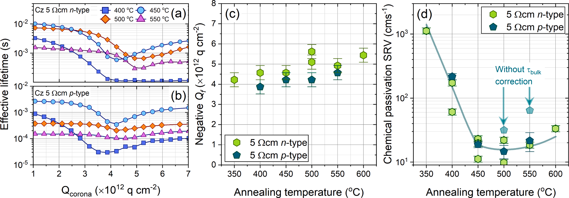
In order to separate the effects of chemical and field-effect passivation of the Al2O3 passivated samples, we subject the samples to corona discharge, whereby controlled amounts of positive charge (e.g., H3O+(H2O)2─8 ions) are deposited onto the surfaces of the Al2O3 films . The choice of positive charge is determined by the charge polarity of the film being investigated. In this case Al2O3 is known to possess a high level of negative charge, thus by depositing enough positive corona charges, we can effectively reduce the net charge to zero. This yields information on the total amount of negative charge in the Al2O3 film, and more importantly, an indication of the ‘interface state density – capture rate’ product (Dit*σn/p) which quantifies the chemical passivation. Fig. 2 (a) and 2 (b) plot the effective lifetime (at Δn = 1015 cm− 3 ) of ALD-grown Al2O3-coated (~20 nm) Cz 5 Ω-cm n-type and p-type (gallium doped) silicon versus the amount of positive corona charge deposited on their surfaces (front and rear) respectively. In both figures, we see an initial decrease in the effective lifetime after subjecting the samples to corona charging, which can be attributed to a reduction in the net field-effect passivation of the films.

Fig. 2. (a) and (b) effective lifetime (at Δn = 1015 cm− 3 ) of ALD-grown Al2O3-coated (~20 nm) Cz 5 Ω–cm n-type and p-type (gallium doped) silicon versus the amount of positive corona charge deposited on their surfaces (front and rear) respectively. Violet squares, blue circles, orange diamonds and purple triangles correspond to samples annealed at 400 ◦C, 450 ◦C, 500 ◦C and 550 ◦C, respectively. (c) Extracted Qf of ALD Al2O3 from corona charge measurements as shown in (a) and (b). (d) Chemical passivation SRV (at Δn = 1015 cm− 3 ) versus annealing temperature with and without a bulk lifetime correction. Green hexagons and aqua pentagons in (c) and (d) correspond to measurements performed on Cz 5 Ω-cm n-type and p-type (gallium doped) silicon, respectively.
4. Conclusion
In this work, we have conducted a thorough investigation of the mechanisms behind the activation temperature-dependent passivation quality of ALD Al2O3 films grown on n- and p-type silicon, separating bulk and surface recombination. We demonstrate that the ambient in which the Al2O3 films are annealed does not appear to have an influence on the level of passivation achieved. We also demonstrate that maximum surface passivation is achieved with a post-deposition annealing temperature of ~ 450 ◦C for 30 min for both n- and p-type silicon. For higher annealing temperatures, the effective lifetime was found to decrease monotonically. However, upon removing the Al2O3 films and re-passivating the surface using a room temperature superacidbased technique, we show that this reduction in passivation is due to degradation of the bulk lifetime. The degrading bulk lifetime dominated the overall effective lifetime, and would yield inaccurate results of the surface passivation quality if this were not understood. By accounting for the reduction in bulk lifetime, in conjunction with corona charging and Kelvin probe experiments, we were able to demonstrate that the chemical passivation of Al2O3 films is stable between annealing temperatures of 450─500 ◦C. In contrast, the negative charge within the films was found to vary with temperature, increasing from –4 × 10¹² qcm− 2 at 350 ◦C to − 5.5 × 10¹² qcm− 2 at 600 ◦C. In conjunction with the thermal stability, we also examined the film thickness dependence on the chemical and field effect passivation. We found that films as thin as 3 nm can achieve maximum chemical passivation when annealed at 450 ◦C, achieving a Dit of ~ 3 × 10¹⁰ eV-1cm− 2 . Thicker films show no further reduction in the Dit, whilst Qf remains constant at ~ 5 × 10¹² qcm− 2 within the 2–30 nm range.
搜索“华林科纳行业观察”小程序查看完整内容,或者加微信13358064333/18106288187。