Abstract:
The main objective of this work is to demonstrate and validate the feasibility of fabricating (Al, In) GaN laser diodes with etched facets. The facets are fabricated using a two-step dry and wet etching process: inductively coupled plasma—reactive ion etching in chlorine, followed by wet etching in tetramethylammonium hydroxide (TMAH). For the dry etching stage, an optimized procedure was used. For the wet etching step, the TMAH temperature was set to a constant value of 80 ◦C, and the only variable parameter was time. The time was divided into individual steps, each of 20 min. To validate the results, electro-optical parameters were measured after each step and compared with a cleaved reference, as well as with scanning electron microscope imaging of the front surface. It was determined that the optimal wet etching time was 40 min. For this time, the laser tested achieved a fully comparable threshold current (within 10%) with the cleaved reference. The described technology is an important step for the future manufacturing of photonic integrated circuits with laser diodes integrated on a chip and for ultra-short-cavity lasers.
1. Introduction
The interest in developing the technology of fabricating laser diode Fabry–Perot resonators by dry or wet etching is almost as old as the modern semiconductor laser diodes themselves. Although the laser bars’ cleavage technology provides parallel and smooth mirrors, it is at the same time expensive, difficult to perform, and noncompatible with on-wafer testing procedures. The main motivation to form the mirrors by etching was and still is the fabrication of short-cavity lasers (short lasers are difficult to cleave) and photonic integrated circuits with fully integrated light sources. There are two fundamental problems related to etched laser mirror technology, namely, the verticality of the mirrors and their smoothness. Verticality requires the etch process to be sensitive to the crystallographic orientation of the facet, and smoothness may be problematic in the case of the etching multilayer structure (varying chemical composition) of the laser diodes.
In the early work of Iga et al. and Miller et al., the possibility of the formation of laser diodes mirrors by wet chemical etching using GalnAsP/lnP lasers was demonstrated. The etched lasers had their threshold currents higher by 50–100% as compared to standard cleaved counterparts. In the next decade, many researchers attempted to use various etching schemes for the GaAs family of lasers. The methods included focused ion beam etching (FIB), reactive ion beam etching (RIBE), chemical-assisted ion beam etching (CAIBE)’s , and reactive ion etching (RIE). The gradual improvement of lasing parameters was observed, concluded by the fabrication of high-power laser diodes with etched mirrors by the RIE method .
2. Laser Diode Preparation
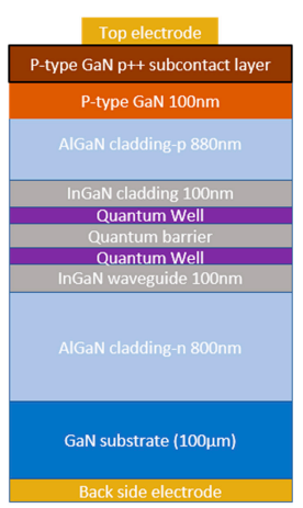
The fully processed laser epi-wafer served as a starting point of the described fabrication process. The design of the laser diode used in this study is shown in Figure 1. The ridge has a width of 2 µm at the base of the mesa structure. The length of all presented devices is the same at 750 µm. More details on the epi-growth of the laser diodes used in this study can be found in the Reference. Part of the epi-wafer was cleaved off to provide reference devices. Additional operations required for etched-facet fabrication are shown in Figure 2. The process starts as the formation of the hard mask consisting of a thin (0.5 µm) layer of photoresist (nLOF 2005) and an over layer of SiO2 with a thickness of 700 nm. The mask was completed with a negative resist (15nXT) with a thickness ofabout 6 um. The mask had the form of a multi-striped pattern, of which the edges weredefined at the localization of the future laser facets. After the exposure and developmentof the top resist, dry etched was performed on the structure in SF plasma to remove theSiO, layer and then in O plasma to remove the thin photoresist at the bottom. Finally dryetching of the semiconductor layers was performed, using ICP RIE with Ar/Cl, plasmaThe depth of the etch was set to be about 4 um deep so that the whole epitaxial structurewas etched through. As a final step , the hard mask was removed by Dimethyl sulfoxide(DMSO) lift-off.

Figure 1. Schematic cross-section of the epitaxial structure of laser diodes used in the present study

Figure 2. Schematic representation of the processing steps: (a) Epitaxial structure processed in theconventional way (20), (b) preparation of the hard mask used to deep etch the laser facet using RlEc) cross-section after the dry etching procedure with an exageerated sloped facet, (d) device after theoptimal wet etch step with a fully formed facet.
The main focus of this work was the optimization of the wet etching stage of the facetprocessing. For that, the same laser chip was used, which was treated by wet etching. Tocontrol this step, the wet etching process was divided into four steps, which allowed thefollowing total times of wet etching to be reached: 0 min, 20 min, 40 min, and 60 min. Aftereach step, the laser was placed in a scanning electron microscope (SEM) for the facet controlSEM imaging), and its opto-electric characteristics were registered. Wet etching was alwaysperformed without using additional masks, as tetramethylammonium hydroxide (TMAH)etches mostly a- and m-planes, and additionally, the c-plane is covered with oxide andundergoes metallization.
3. Results and Discussion
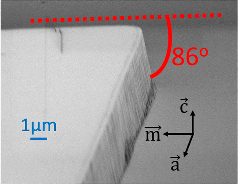
Before starting the main process of facet fabrication, the calibration of the dry etchingprocedure was conducted. Reactive ion etching is the most common method of etchingc-plane-oriented GaN-based layers. The example of our optimized ICP-RIE procedureis shown in Figure 3a. The etching was done on a laser epitaxial structure but withoutprocessing (no contacts or insulation layers).


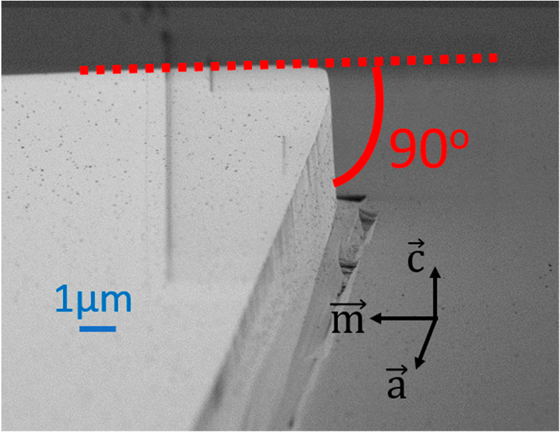
Figure 3. SEM images of the test sample of the laser epitaxial structure (a) after reactive ion etching, (b) the same edge after RIE and TMAH wet etching.
Figure 3a shows that the smoothness of the etched facetis good, but the inclinationangle is about 86°, which is not sufficient to form an effective laser cavity. The estimation ofthe inclination of the vertical" facet was measured for multiple samples. The tools used forthis procedure were a stylus profilometer, SEM, and simple trigonometric calculations. Themethod was as follows. Firstly, the value of the height of the deep etch was measured bya stylus profilometer. Next, the specimen was cleaved along the easy-cleavage m-plane andplaced in the SEM chamber. The sample was positioned so that the value of the height ofthe deep etch reproduced the result from the profilometer. This ensured the correctness ofthe SEM imaging and allowed us to determine the angle of the "vertical" facet inclinationThree different etching procedures were performed for this set of parameters (85 0C20 min) to check if the results were repeatable. For each etching procedure, there wereabout 20 measurements of angles. The average is the value presented in this work. Thedeviations are within the estimated accuracy of this measuring method (about 1%). Theobtained value of 86° is in agreement with previous literature reports .
TMAH Etching
In the developed wet etching procedure, 25% wt. aqueous TMAH solution was usedThe solution was kept at a constant temperature of 80°C and stirred during all process stepsAs shown before (1729,30l, under similar conditions, etching is very fast for a-planes, veryslow for m-planes, and does not occur (in a measurable way) for the c-plane. Since the laseldiodes are oriented in the same direction as cleaved devices, the slowly etched m-planeswill create device facets. Strict crystallographic orientation of these facets provides ourdevices with the high-quality resonance cavity needed for Fabry-Perot edge emitting lasers.
4. Conclusions
This paper presents the fabrication of (Al, In) GaN laser diodes with etched facets grown on bulk GaN substrates. The facets were obtained by a two-step etching process: dry etching by reactive ion etching followed by wet etching in TMAH. The work focused on optimizing the duration of the process and its effect on facet morphology and optoelectronic parameters.
搜索“华林科纳行业观察”小程序查看完整内容,或者加微信13358064333/18106288187。
上一篇: 硅氧化铝表面钝化的激活:分离体和表面效应
下一篇: 4H 碳化硅晶圆的化学机械抛光