4H silicon carbide (4H-SiC) holds great promise for high-power and highfrequency electronics, in which high-quality 4H-SiC wafers with both global and local planarization are cornerstones. Chemical–mechanical polishing (CMP) is the key processing technology in the planarization of 4H-SiC wafers. Enhancing the performance of CMP is critical to improving the surface quality and reducing the processing cost of 4H-SiC wafers. In this review, the superior properties of 4H-SiC and the processing of 4H-SiC wafers are introduced. The development of CMP with chemical, mechanical, and chemical– mechanical synergistic approaches to improve the performance of CMP is systematically reviewed. The basic principle and processing system of each improvement approach are presented. By comparing the material removal rate of CMP and the surface roughness of CMP-treated 4H-SiC wafers, the prospect on the chemical, mechanical, and chemical–mechanical synergistic improvement approaches is finally provided.
1. Introduction
4H silicon carbide (4H-SiC) is emerging as a dominant semiconductor material to enable the ever-increasing deployment of high-power, high-frequency, high-temperature and radiation-resistant devices.Compared with silicon (Si)-based the highpower devices based on 4H-SiC have the advantages of higher power density, lower power consumption, and smaller size. As shown in Figure 1, the devices using 4H-SiC have been successfully utilized in a series of fields such as electric vehicles, railways, uninterruptible power supplies (UPS), high-voltage grids, and 5G communications.For example, the powerconversion efficiency of the G2020 series 4H-SiC-based UPS developed by Toshiba has reached 98.2%.Toyota has replaced Si-based PIN diodes with 4H-SiC-based Schottky-barrier diodes in the DC converters of hybrid electric vehicles, leading to 30% reduction of energy loss and 0.5% increase of conversion efficiency. Mitsubishi Electric Corporation has equipped a 4H-SiC power module in the train traction inverter of the N700S Shinkansen subway, enabling the switching loss and volume of the system to be reduced by 55% and 40–65%, respectively. The promising applications of 4H-SiC have boosted the requirements for high-quality 4H-SiC wafers. Since the surface quality of 4H-SiC wafers significantly affects the quality of epitaxial 4H-SiC (homoepitaxy) or GaN (heteroepitaxy) and thus the quality of final devices, the processing of the surface of 4H-SiC wafers is crucial to the success of 4H-SiC in semiconductor industry.
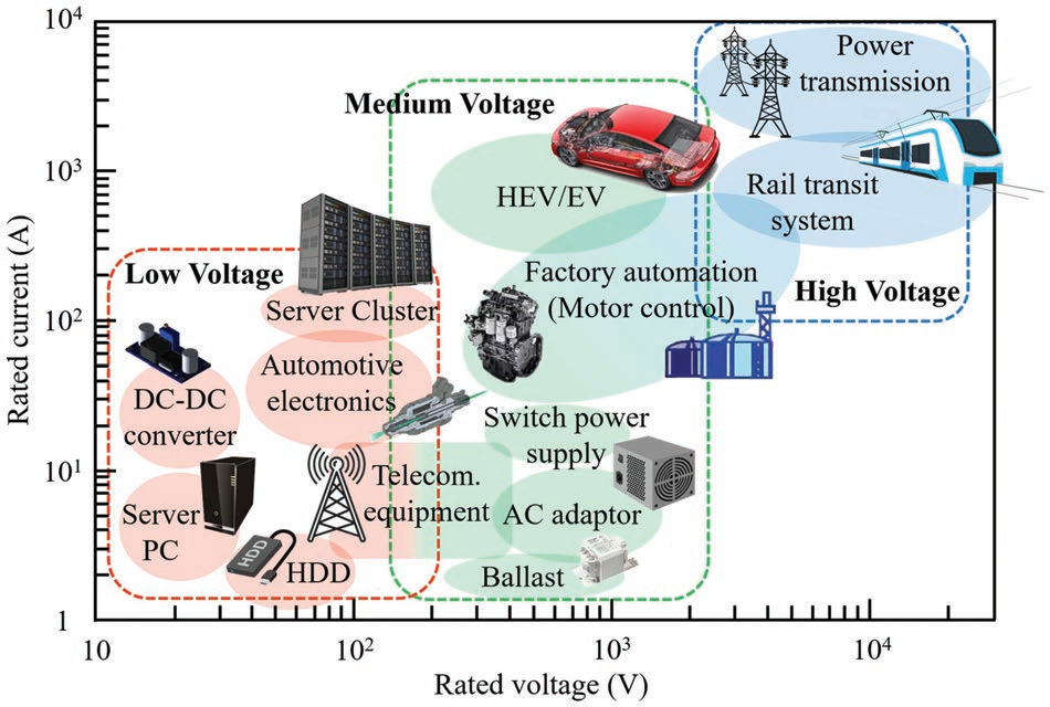
Figure 1. Major application fileds of the electronic devices based on 4H-SiC.
Chemical–mechanical polishing (CMP) has been developed as a state-of-the-art technology to achieve global planarization of the surface of 4H-SiC wafers. During CMP, the surface of a 4H-SiC wafer undergoes cycles of chemical oxidation and mechanical removal under the interaction among the 4H-SiC wafer, polishing slurry, and polishing pad.Given the high hardness and strong chemical inertness of 4H-SiC, the CMP of 4H-SiC wafers faces the challenges of long processing time, high cost, and low technical flexibility.In order to improve the surface quality and processing efficiency of 4H-SiC wafers, researchers have been investigating various approaches.
2. Properties and Manufacturing of 4H-SiC Wafers
2.1. Properties of SiC
The bonding between Si and C is shown in Figure 2a. The bond length and binding energy of SiC are ≈1.89 Å and ≈289 kJ mol−1 , respectively. They give rise to the extremely high hardness and strong chemical stability of SiC.SiC has more than 200 homogeneous polymorphs, of which 3C-, 4H-, and 6H-SiC are rather common. The structures of 3C-, 4H-, and 6H-SiC are schematically shown in Figure 2b. The letters A, B, and C denote sites occupied by SiC bilayers in a hexagonal close-packed structure. The stacking sequences of SiC bilayers of 3C-, 4H-, and 6H-SiC are ABC, ABCB, and ABCACB, respectively. Figure 2c displays crystal directions and planes of hexagonal 4H-SiC. The planes with the direction of [0001] and [0001] are often called the Si face and C face, respectively.
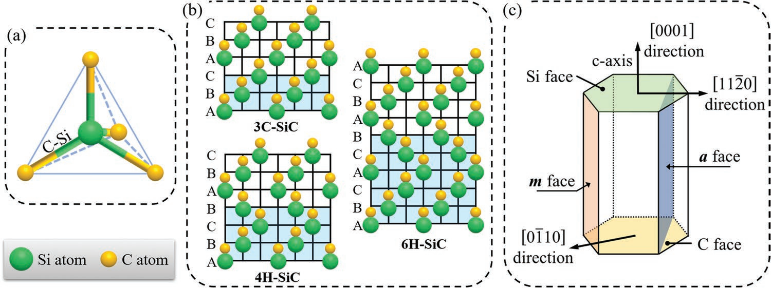
Figure 2. Schematic diagrams of a) tetrahedron structure formed by SiC bonds, b) stacking sequence of SiC bilayers in 3C-, 4H-, and 6H-SiC, and c) major crystal faces in hexagonal SiC.
Given the same bonding between Si and C, 3C-, 4H-, and 6H-SiC have similar mechanical and chemical properties. However, due to the different stacking sequences of SiC bilayers, the electrical properties of 3C-, 4H-, and 6H-SiC are different from each other. As shown in Figure 3, the critical electric field, bandgap energy, saturated electron velocity and electron mobility of 4H-SiC all prevail over those of 3C- and 6H-SiC, which makes 4H-SiC being the ideal polymorph of SiC for the applications of high-power, high-frequency, and high-temperature electronics.Therefore, we focus on the improvement of the CMP of 4H-SiC in this review. It should be noted that early work was mainly related to the CMP of 6H-SiC. Because of the similar mechanical and chemical properties of 4H- and 6H-SiC, the mechanical and chemical improvements for the CMP of 6H-SiC wafers are conducive to the improvements of the CMP of 4H-SiC wafers.
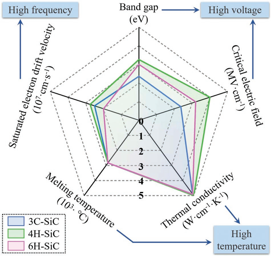
Figure 3. Comparison of physical properties and electronic properties of 3C-, 4H-, and 6H-SiC.
2.2. Manufacturing of 4H-SiC Wafers
As shown in Figure 4, the processing procedure of a 4H-SiC wafer mainly includes wire sawing, edge rounding, grinding, lapping, and CMP.Firstly, a 4H-SiC boule is sliced into wafers during multi-wire sawing. Each 4H-SiC wafer is then mounted on a grinding chuck. A profile rounding wheel rounds the wafer edge according to the product’s specifications. Grinding is subsequently carried out to rapidly reduce the thickness of the wafer. The wafer further undergoes a series of lapping processes to increase the parallelism of the surfaces and remove surface/sub-surface damage induced by the wire-sawing. Finally, CMP is used to improve the flatness and achieve an atomically smooth surface of the wafer.
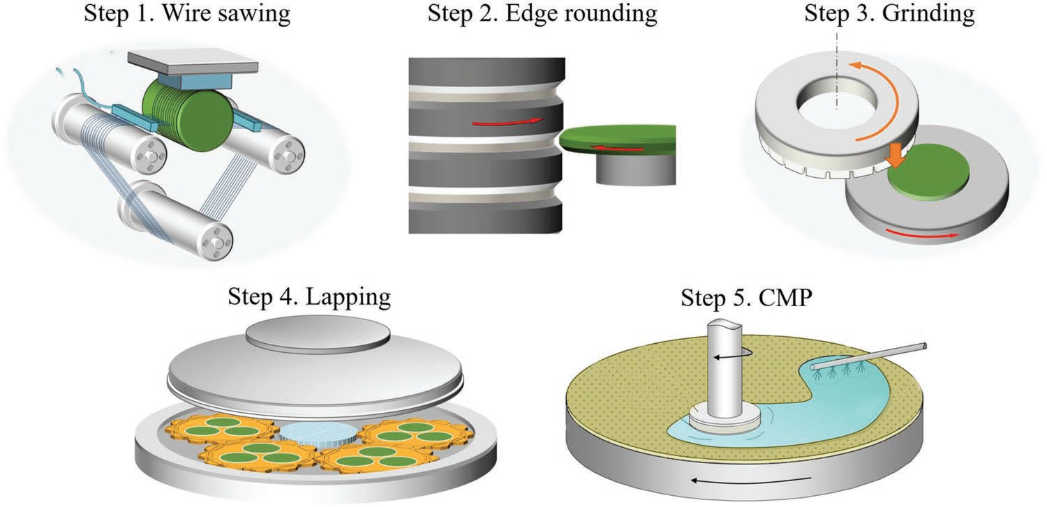
Figure 4. Schematic diagram of typical manufacturing procedures of 4H-SiC wafers, including wire sawing, edge rounding, grinding, lapping, and CMP.
3. Status and Challenges of the Chemical– Mechanical Polishing (CMP) of 4H-SiC Wafers
3.1. Traditional CMP Methods
CMP appeared in the mid-20th century, which had attracted great attention owing to its capability of planarizing both glass and metal. When IBM corporation first introduced CMP to the manufacturing of integrated circuits in 1988, CMP began to be widely used in the processing of semiconductor wafers because both the global and local planarization can be achieved simultaneously. As shown in Figure 5, a CMP system mainly consists of three parts: the polishing slurry, the polishing pad, and the polishing machine containing components such as the polishing head and polishing plate. In a typical CMP process, a wafer is bonded to the bottom of a polishing head. The polishing slurry with specific functions is continuously dripped to the surface of the polishing pad. The wafer, polishing slurry, and polishing pad are in close contact under certain pressure and rotated with the polishing head and polishing plate. During the relative motion, the surface of the wafer and the polishing slurry chemically react. The reaction product is removed by the mechanical interaction among abrasives in the polishing slurry, the polishing pad and the wafer. The global and local planarization of the wafer is ultimately realized by the cycling of the chemical reaction and mechanical removal processes.
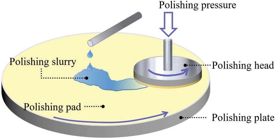
Figure 5. Schematic diagram of a typical CMP system, including polishing head, polishing plate, polishing slurry, and polishing pad. During CMP process, the 4H-SiC wafer, polishing slurry, and polishing pad are in close contact under certain pressure and rotated with the polishing head and polishing plate.
4. Conclusions and Prospects
In summary, we have reviewed the CMP of 4H-SiC wafers. Although CMP has achieved great success on the processing of 4H-SiC wafers, chemical, mechanical, and chemical– mechanical synergistic improvement approaches have been proposed to enhance the MRR of CMP, and improve the surface quality of 4H-SiC wafers.
For chemical improvement approaches, the Fenton-like reaction may improve the efficiency of CMP with low cost. But residual Fe ions after CMP pose a challenge for postCMP cleaning. For the emerging PCMP, the long-term stability of the photocatalyst in the slurry is an important issue. Furthermore, the temperature fluctuation induced by long-time UV irradiation during PCMP should be monitored and controlled.
For mechanical improvement approaches, alumina- or ceriabased MAS and core–shell abrasive particles have been regarded as excellent components for novel polishing slurries. However, the dispersion stability of the nanoparticles needs to be optimized to increase the reliability and reproducibility of the highvolume fabrication of MAS or core–shell abrasive slurry.
To date, the emerging CMP efficiency enhancement technologies are still in the industrial validation stage of moving from the lab to the fab. Currently, PCMP and MAS technologies are showing potential in the industrial standard. In terms of leading on a research level, PAP and ECMP are considered to be more forward-looking.
搜索“华林科纳行业观察”小程序查看完整内容,或者加微信13358064333/18106288187。
下一篇: EUV光学器件纳米层的热稳定性