1.1Thin films
A coating is a layer of a material that covers the surface of an object and that has a thickness that is much smaller than the extension of the layer in the two dimensions parallel to the surface. Generally, coatings are used to introduce functionalities by modifying properties and adding extra ones to a material. Well-known is the coating of materials simply for decorative purposes. Paint layers form one of the first and most used examples of that type of coating. The precise origins of the application of paint are unknown, but what is clear, is that they must be very old. The oldest documented figurative paintings are estimated to be at least 40.000 years old, which is in the Paleolithic, also known as the old stone age. The non-figurative paintings go back in time even before the habitation of modern humans in Europe3 . Thinner classes of coatings are nowadays referred to as “thin films”. The first known thin metallic films are more than 5000 years old, which puts them in the middle bronze age. They were found in Egyptian tombs as the decorative gilding of death masks, sarcophagi and burial attributes. In time, the types of thin films and their applications have grown into a wide variety and they can be found all around us, making them an essential part of today’s products and technology. Common applications of thin metal films are to be found in household mirrors that consist of a glass plate covered at the rear side by a thin reflective metal film, and in the protective layers on touch screens of laptops and smartphones. For many practical applications, thin metal coatings are deposited on objects by straightforward techniques, such as hot-dip galvanizing, thermal spraying, electroplating and sherardizing.
In order to understand the wetting properties of thin films, we need to inspect them from a thermodynamic perspective. Driving the wetting or dewetting is the reduction of the total surface and interface free energy of the film-plus-substrate system. The surface free energy quantifies the free-energy investment that is required to form a unit area of that surface out of a continuous, three-dimensional bulk arrangement of the same material. This accounts for the loss of interatomic or intermolecular interactions across the interface, which may be partly compensated by rearrangements at and close to the surface. Nevertheless, for most materials, the surfaces and interfaces come with positive free energies, which means that the materials tend to minimize the areas of their surfaces and interfaces.

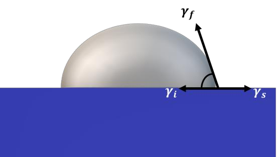
Figure 1The equilibrium shape of a material that covers a substrate incompletely, with a contact angle θ>0, corresponding to dewetting, as described by the Young-Laplace equation.
where γ𝑠 , γ𝑓 and γ𝑖 are free energies per unit area of the surface of the substrate material, the surface of the thin film material and their interface, respectively, and 𝜃 is the equilibrium contact angle (Fig 1). When 𝜃 > 0, the equilibrium solution corresponds to a geometry with incomplete coverage of the substrate by the overlayer or, in other words, to dewetting. When, on the other hand, the stability condition is satisfied;
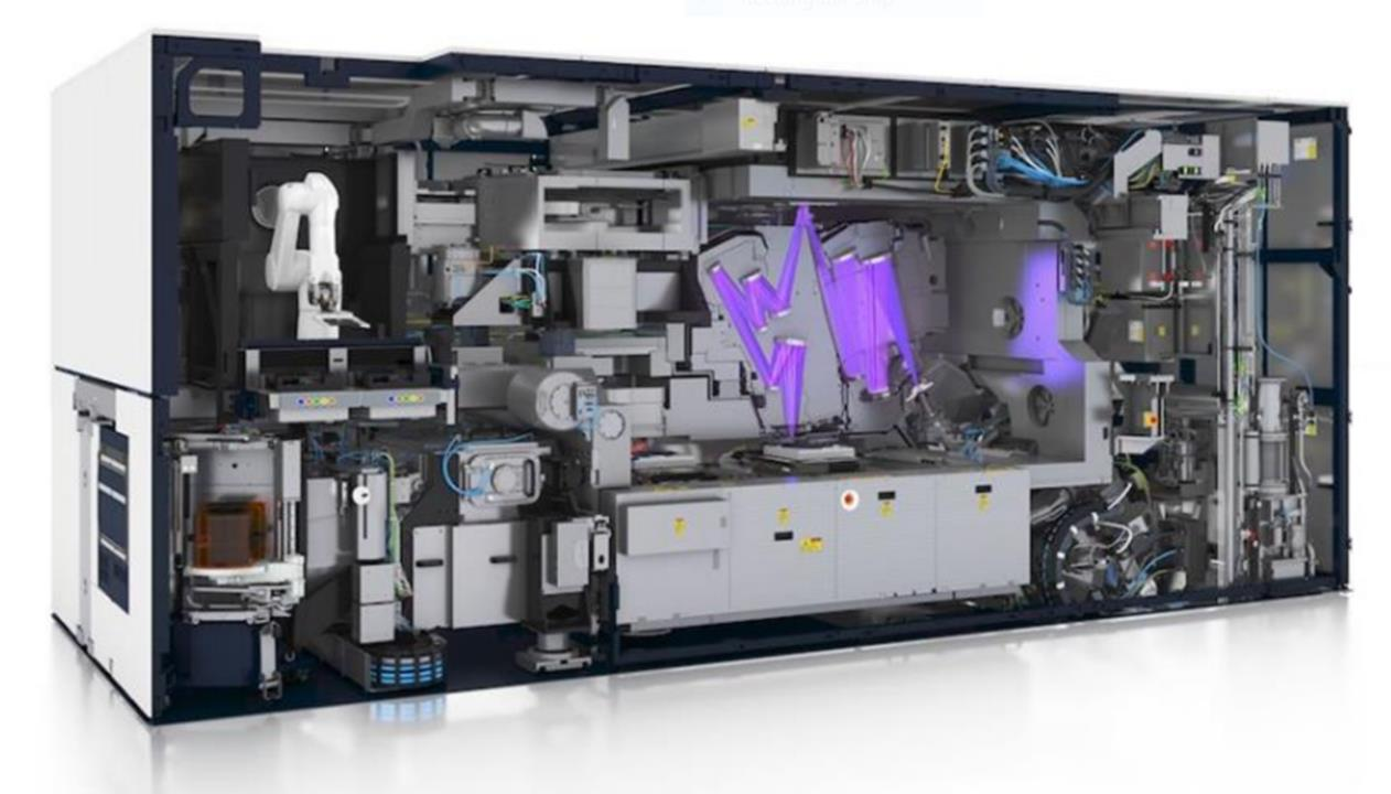
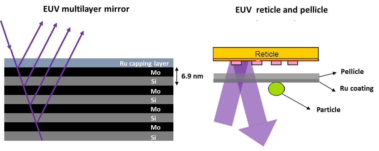
A special class of applications in which dewetting can be problematic is formed by the thin film components that are used in state-of-the-art machines for photolithography with extreme ultraviolet (EUV) light (Figure 1.2). These machines are used for the production of the most refined processor and memory chips to date. In the context of this technology, ‘EUV’ refers to a wavelength of 13.5 nm. Examples of critical components of these machines that contain thin films are multilayer mirrors and pellicles (Figure 1.3). The mirrors are curved and act as lenses. They are used instead of conventional refractive optics that are of no use at 13.5 nm, because of the extreme absorption they would introduce at this wavelength. The curved mirrors are decorated with a multilayer stack in order to reach an acceptable fraction of reflected light at or close to normal incidence. In these stacks, each interface contributes a small amount to the reflected light amplitude, while a careful choice of the thicknesses of the layers ensures constructive interference of all partial reflections at normal incidence. At 13.5 nm, Si and Mo are used for these multilayer structures in view of their combination of acceptable absorption and relatively high optical contrast at this wavelength. When a precise period of 6.9 nm is chosen for each bilayer, the reflectivity of a single multilayer mirror can, in principle, be as high as 74%55 , but in practice, recorded values reach up to 69.5%56. EUV pellicles are ultrathin, freestanding membranes. These protect other elements in the lithography machines, such as the reticles – these are the masks with the ‘blueprints’ of the semiconductor device that is produced – that can become useless as the consequence of only a single particle landing in the ‘wrong’ place. The pellicles need to combine a high transmission for the EUV light, in order to minimize the loss of this light, with a high infrared emissivity, in order to limit the heating of the pellicle itself that results from the absorbed fraction of the EUV light.

Figure 1.2 Artist impression of an ASML EUV lithography machine. The optical trajectory of the EUV light is highlighted in purple, with the EUV source position on the far right, the reticle in the upper part and the illuminated semiconductor wafer in the center of the picture (Image source: ASML).

Figure 1.3 Schematic illustrations of a multilayer EUV mirror and of the use of an EUV pellicle to protect the reticle (mask) from the arrival of particles that would otherwise be imaged sharply on the semiconductor wafer in the lithography process. Both multilayer mirrors and pellicles are typically covered by a capping layer, usually in the form of a Ru film with a thickness in the order of a few nanometers.
The second chapter of this thesis will address the growth and stability of elemental films of Mo and Ru and of Ru-Mo bilayers on Si substrates with a native oxide. The thermal stability, especially with respect to the grooving of grain boundaries and the de-wetting of the ultrathin films, is investigated by bringing the films to elevated temperatures and inspecting the result by various forms of microscopy and spectroscopy.
Chapter 3 will review the literature about more radical, possible solutions to the grooving behavior, introduced by the grain boundaries of thin, polycrystalline metal films. Most importantly, we will discuss possibilities to produce films of Mo and Ru with no grains at all, in the form of a metallic glass. For this, it is essential to familiarize ourselves with the thermodynamics and the evolutionary dynamics of amorphous and polycrystalline metal alloys. In addition to this, we will briefly review the fabrication methods, properties and limitations of such metallic glasses.
1.2 Experimental methods
A Polyteknik Flextura M506 S system was used in the NanoLab facility of our neighbor institute AMOLF, for the sputter deposition58 of all thin films in this work. In contrast to Ru-Mo growth studies reported in the literature, our substrates were kept at room temperature. All films were deposited on p-doped Si(100) substrates; the native oxide on these substrates was not removed prior to deposition. For the production of thin MoxRu100- x alloy films, Mo and Ru were co-deposited from separate sources by RF and DC sputtering, respectively. We used different types of power supplies for the two metals for practical reasons, but we do not expect this to influence the results significantly. The base pressure of the sputter deposition system was 1 x 10⁻⁷ mbar and the argon (Ar) pressure was 2 x 10- 3 mbar or higher during the deposition. In addition to the alloy films, also regular films of pure molybdenum and pure ruthenium were deposited by DC sputtering. During deposition, the substrates were rotated, in order to optimize the homogeneity of the deposition.
Characterization
Measurements of the thicknesses of the deposited metal films were carried out in the following way. Prior to metal deposition, which was usually done simultaneously on multiple substrates, one of these substrates was partly coated by a photoresist film. After the metal deposition, the resist was washed off by acetone and isopropanol and this cleaning procedure also removed the deposited metal film from those parts of the substrate that had first been coated by the resist, while the metal film on other parts of the substrate stayed in place and remained unaffected. This procedure enabled us to accurately measure the height difference between the bare regions where the resist was removed and the regions that had not been coated by the resist and that were covered by the thin metal film. These height difference measurements were done by use of a profilometer and by atomic force microscopy (AFM). This provided us with accurate measurements of the film thicknesses. Samples used to measure the film thickness were not utilized for further experiments to avoid possible contamination from the employed chemicals and their residues. The films used in this thesis had thicknesses typically ranging from 4 to 30 nm.
We used AMOLF’s FEI Verios 460 SEM system, with a Schottky field electron gun, for the inspection of substrates and thin films with scanning electron microscopy. The SEM images were taken at an electron energy of 5 keV and a beam current of 100 pA, unless indicated differently, and the samples were placed at approximately 4 mm distance from the analyzer. For all SEM images, we used the immersion field mode, in order to optimize the spatial resolution.
Transmission electron microscopy (TEM)68 measurements were performed at the Zernike Institute for Advanced Materials of Groningen University. For this purpose, cross-sectional specimens were prepared in Groningen, with an FEI Helios G4 CX dual beam system at 30 kV ion energy and polished at 5 keV and 2 keV to remove residual surface damage. These specimens were analyzed with a double-aberration-corrected FEI Themis Z scanning transmission electron microscopy (STEM) system at 300 kV. High-angle annular dark-field (HAADF) STEM images were recorded with a probe current of approximately 200 pA, at a convergence semi-angle of 21mrad and with HAADF collection angles of 61–200 mrad. EDX spectral imaging was performed with a probe current of 1 nA, where the spectra were recorded with a Dual-X system, providing in total 1.76 sr EDX detector.
搜索“华林科纳行业观察”小程序查看完整内容,或者加微信13358064333/18106288187。
上一篇: 4H 碳化硅晶圆的化学机械抛光