Sputter epitaxy is a low-cost process suited for the deposition of group-III-nitride semiconductors and allowing the deposition on large substrate areas at lower growth temperatures than in metal–organic vapor phase epitaxy (MOVPE). Highquality AlN, AlGaN, and GaN epitaxially grown on Si(111) substrates by reactive magnetron sputtering are demonstrated and details on process parameters are given. With an ammonia-based reactive sputtering process in a high-purity environment, AlN can be grown with high crystalline quality comparable to the best MOVPE-grown samples regarding twist and tilt and with a very low surface roughness, free of the typical columnar structure of sputtered AlN and pits. Also AlGaN, typically required for strain engineering of GaN layers grown on Si, can be grown in the entire compositional range by co-sputtering of Al and Ga. Thin undoped buffer layer samples show high breakdown field strengths well above 2.5 x10⁶ V cm- 1 and demonstrate the possible use for field effect transistor (FET) buffer layers.
1. Introduction
The deposition of compound semiconductors with device quality has been long time a domain of molecular beam epitaxy (MBE) and metal–organic vapor phase epitaxy (MOVPE) of which the latter is today’s most widely spread technology for the growth of optoelectronic and electronic device layers. Apart from this, deposition techniques such as magnetron sputtering are well established for the deposition of amorphous to textured thin films but rarely for epitaxial layers of high quality. For lowering the cost of thin-film growth, magnetron sputtering is an interesting technique as it is easily scalable and operates at a lower temperature as MOVPE, enabling lower thermal stresses of heteroepitaxial films. Due to the lower growth temperatures required, it potentially also eases, e.g., integration with Si complementary metaloxide-semiconductor (CMOS) technology. In the past decade, Hiroshi Fujioka and his group first demonstrated high-quality GaN-based layers by pulsed laser epitaxy (PLE) and then by pulsed sputter epitaxy (PSE). However, there were only a few other groups active in this field and similar results are not yet reported. When looking for conditions to obtain high-quality films by sputter epitaxy there is a lack of information about targets, gases, and sputtering parameters used. Here we present a study of the basic parameters required to achieve high-quality AlN and AlGaN layers and the impact of growth parameters on GaN films using reactive magnetron sputtering. As cost is one important issue, we have developed heteroepitaxial growth on low-cost Si(111) substrates, typical for high-power device applications. Nevertheless, the results presented can also be transferred to the growth on sapphire by optimization of the seeding layer.
2. Results
2.1. Base Pressure
In a first test series, we investigated the impact of the base pressure on the quality of AlN thin films on Si(111) using a nitrogen–argon mixture and a 2’’ 6N5 Al target. Initially, a system without load-lock and with a typical base pressure of 5 x10- 3 mbar was used. Another test was performed in the same system using an extended evacuation sequence to reach a base pressure of 5 x10⁻⁴ mbar. Later, AlN growth was investigated in another system with a load-lock reaching a lower base pressure of 5 x10⁻⁷ mbar, and finally, our custom-made system with a load-lock and a base pressure of 5x10- 9 mbar was compared. In the first two systems, the substrate was wet and chemically deoxidized prior to loading and heated to 750 °C. Figure 1 shows Θ-2Θ X-ray diffraction (XRD) scans in a range where intensity from an AlN(0002) diffraction peak is expected. While for growth under poor vacuum conditions, none or only multiple peaks are observed a single peak that gets narrower is found for high to ultra-high vacuum conditions confirming the importance of the quality of the vacuum. For high-rate sputtering, these conditions might be less strict but seeding then remains a problem as we will show in the next section.
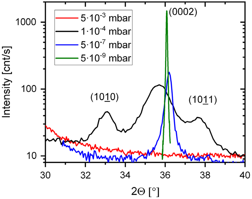
Figure 1. X-ray diffraction (XRD) Θ-2Θ scans around the (0002) AlN diffraction peak for samples grown at different base pressures of the sputtering system.
2.2. AlN
To start epitaxial growth on Si, GaN is not well suited due to the formation of a Ga–Si alloy at elevated temperatures leading to melt-back etching. To avoid this problem the typical layer initiating group-III-nitride growth on Si is AlN. To find start conditions for the sputtering of AlN on Si we did some pre-tests on AlN templates. With these basic sputtering parameters we then adopted a process similar to MOVPE and MBE processes where it is common to start growing with a short Al-pretreatment before opening the nitrogen source. It is found that also for sputtered AlN on Si this is a beneficial procedure: Figure 2 shows the dependence of the XRD in-plane (1010) and out-of-plane (0002) full width at half maximum (FWHM) on the gas mixture used and on the nominal thickness of the Al-pre-treatment for AlN grown at 900 °C. For the initial sputtering of AlN on Si, a supply of Ar þ N2 leads to better XRD values than an Ar þ NH3 supply. The ideal nominal thickness of the Al-pre-treatment in the Ar þ N2 case corresponds to about 2 Å, equivalent to approximately a monolayer of aluminum. In atomic force microscopy (AFM) (Figure 3a), one finds that the resulting surface morphology is very different for the different conditions.
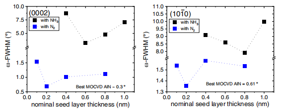
Figure 2. XRD ω scans of the AlN (0002) and (1010) reflections for different thicknesses of the metallic Al-predeposition on Si at 900 °C. Using nitrogen an about a monolayer thick deposition is required while, when using ammonia, the thickness is much higher and the quality achieved much lower which we attribute to the strong reactivity of ammonia with Si leading to the formation of SiN before full AlN coverage of the substrate.
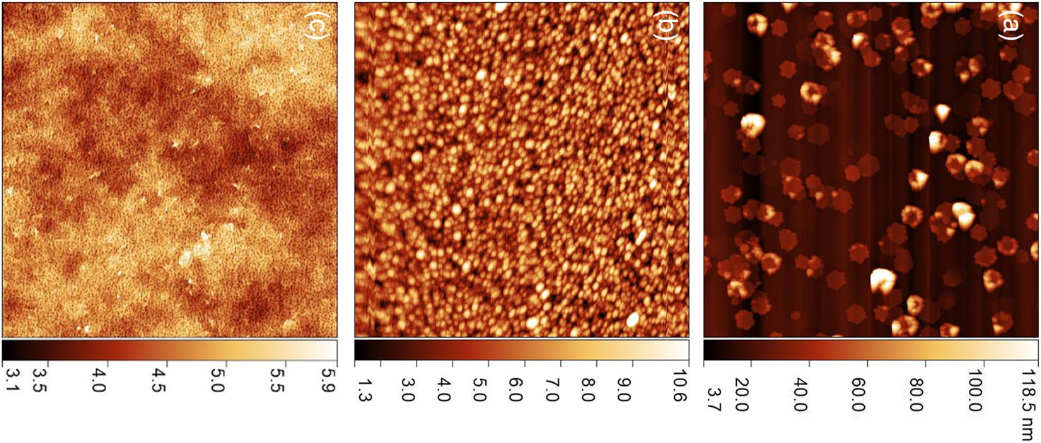
Figure 3. 5 x 5 μm2 atomic force microscopy (AFM) images a) of AlN grown on Si using ammonia leading to a rough surface. b) Using nitrogen instead of ammonia leads to a smoother but still columnar structure. c) The combined process with first a layer grown under nitrogen and then ammonia leads to an excellent morphology and crystalline quality. The scale bar is in nm.
From pre-tests for optimizing basic growth parameters on AlN templates we actually found that the growth of AlN using Ar þ NH3 leads to smooth layers. But here ammonia does lead to poor surfaces and two AlN contributions or a single very broad AlN signal in XRD measurements (not shown here). We interpret the difference between nitrogen and ammonia by a higher reactivity of ammonia with Si leading to the formation of SiN and blocking a good epitaxial relationship between AlN and Si. For a nominally thicker Al-pre-treatment, this nitridation process likely can be reduced. Nevertheless, even for the best layer achieved with ammonia, the crystalline quality and morphology are too low for further device layer growth.
While the crystalline quality is good for AlN grown with nitrogen, the surface morphology of such samples reflects the typical columnar structure of AlN sputtered with nitrogen which is not suited for smooth interfaces (Figure 3b).
In the NH3-based growth process, the growth temperature has an impact on the crystalline quality which we tested by growing AlN on MOVPE-grown AlN/sapphire templates. The crystalline quality improves slightly with increasing growth temperature and is of nearly equal quality above 700 °C. The surface morphology is best for layers around 900 °C (Figure 4). At low temperatures, small holes exist in the surface and the structure shows a more pronounced grain structure. This can be understood by the low surface mobility of Al at these temperatures. The surface roughness gets smoother up to an optimum temperature of around 900 °C and again increases at temperatures of 1000 °C where small holes are found.
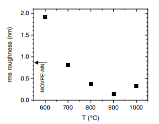
Figure 4. Surface roughness from 3 x3 μm2 AFM scans for AlN grown on AlN templates using ammonia at different temperatures different temperatures showing a minimum at 900 °C thermocouple reading. The typical RMS roughness of metal–organic vapor phase epitaxy (MOVPE) grown layers is indicated by an arrow.
2.3. AlGaN
AlGaN layers are important as active layers of electronic devices, e.g., field effect transistors (FETs)or for strain engineering, e.g., when using a (step) graded AlGaN buffer.Little has been reported on the growth parameters of AlGaN up to now.Here the growth of AlGaN has been performed by co-sputtering from an Al and Ga target using an NH3-based process. The layers were sputtered in one growth process after the growth of an AlN on Si buffer at a temperature of 800 °C and an ammonia flow of 20 sccm, first with a constant power of the Al-target of 200 W while decreasing the power of the Ga-target from 200 to 20 W. It should be noted that the best results for AlN are obtained with an ammonia flow of 20 sccm while for GaN 40 sccm is optimum to obtain smooth surfaces.
A linear dependence of the composition is found until an Al concentration of 73% (Figure 5a). As the Ga-target cannot be operated at powers below 20 W, we increased the plasma power of the Al-target to 300 W (Ga: 20 W) and then achieved an Al-concentration well above 80%. For the growth of most device structures, this concentration range is sufficient. Figure 5b shows a Θ- 2Θ XRD scan of Al0.73Ga0.27N on AlN. The oscillations between and around the two (0002) diffraction peaks indicate a very high smoothness of the interface and the surface of the sample.
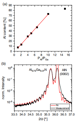
Figure 5. a) Composition of AlGaN in dependence of the power ratio. b) The bottom viewgraph shows a Θ-2Θ XRD scan of an AlGaN layer with 73% of Al with well pronounced thickness interference fringes indicating very smooth interfaces.
In a different set of samples, we investigated the impact of growth temperature and observed that the Ga-content decreases when increasing the growth temperature which we assign to Ga desorption. Consequently, when growing at different temperatures one has to evaluate the composition at different temperatures.
3. Summary
We have demonstrated the magnetron sputter epitaxy of AlN, AlGaN, and GaN and report on details of the dependence of the layer quality on major sputtering parameters. While optimization is still required for GaN growth the present results demonstrate the high potential of this method as, e.g., the quality of AlN on Si layers is hard to achieve in MOVPE and all other layers grown on Si are of similar crystallographic quality as similar layers grown by MOVPE. Most important is the finding that ammonia instead of nitrogen as reactive gas leads to a much higher quality of the layers paving the way to commercial applications. Already now the present layer quality is sufficient for templates for MOVPE overgrowth and likely soon for complete device structures.
4. Experimental Section
All layers, except for a first basic study, were grown in a custom-made magnetron sputter system with two 4’’ magnetrons for Ga (7N5) and Al (6N5) and several 2’’ magnetrons for other materials. A 2’’ or 4’’ substrate was mounted upside down underneath a resistance heater (TMax. ¼ 1000 °C). The grounded substrate was placed at a distance of ≈15 cm between most magnetrons. This configuration was chosen as the metallic Ga target liquefies at 29 °C, which is difficult and impossible to fabricate and handle in a process where targets are subjected to signifi- cant amounts of heat. Here, solid Ga was loaded into an electropolished Mo crucible and then molten by heating to achieve a homogenous coverage within the crucible. During sputtering, the Ga target was cooled to - 20 °C, and all other magnetrons were held at þ18 °C through external chillers. As gases got purified, Ar, H2, N2, and NH3 were used in the chamber which can reach a base pressure of 5 x 10⁻⁹ mbar. Sputtering was performed under 200 W pulsed DC conditions, where a pulse length of 200 μs with a duty cycle of 0.5 was used. Growth was performed at a pressure of 5 x10⁻³ mbar on p-Si(111) substrates which were heat treated for 6 min at 900 °C prior to growth under hydrogen at similar chamber pressure. Ar was always set at a constant flow of 100 sccm and N2 (90 sccm) or NH3 (different flows) added. Temperatures given here corresponded to thermocouple readings and were≈30 K higher than the surface temperature as determined by in situ temperature measurements with a Laytec EpiR TT, which is also useful for fast optimization of the growth process.
搜索“华林科纳行业观察”小程序查看完整内容,或者加微信13358064333/18106288187。
上一篇: EUV光学器件纳米层的热稳定性