Abstract:
Gallium nitride is a wide-direct-bandgap semiconductor suitable for the creation of modern optoelectronic devices and radiation tolerant detectors. However, formation of dislocations is inevitable in MOCVD GaN materials. Dislocations serve as accumulators of point defects within space charge regions covering cores of dislocations. Space charge regions also may act as local volumes of enhanced non-radiative recombination, deteriorating the photoluminescence efficiency. Surface etching has appeared to be an efficient means to increase the photoluminescence yield from MOCVD GaN materials. This work aimed to improve the scintillation characteristics of MOCVD GaN by a wet etching method. An additional blue photo-luminescence (B-PL) band peaking at 2.7–2.9 eV and related to dislocations was discovered. This B-PL band intensity appeared to be dependent on wet etching exposure. The intensity of the B-PL was considerably enhanced when recorded at rather low temperatures. This finding resembles PL thermal quenching of B-PL centers. The mechanisms of scintillation intensity and spectrum variations were examined by coordinating the complementary photo-ionization and PL spectroscopy techniques. Analysis of dislocation etch pits was additionally performed by scanning techniques, such as confocal and atomic force microscopy. It was proved that this blue luminescence band, which peaked at 2.7–2.9 eV, is related to point defects those decorate dislocation cores. It was shown that the intensity of this blue PL band was increased due to enhancement of light extraction efficiency, dependent on the surface area of either single etch-pit or total etched crystal surface.
1. Introduction
Gallium nitride (GaN) is a wide-direct-bandgap semiconductor suitable for the creation of modern optoelectronic devices and radiation-tolerant detectors. This material can be synthesized using various crystal growth methods. Metalorganic chemical vapor deposition (MOCVD) is commonly used for growing of rather thin GaN crystal layers on various substrates. However, the density of dislocations in these crystals can reach 1010 cm−2 , while small density of vacancies is inherent to MOCVD materials. Modern growth methods of bulk GaN crystals, such as ammonothermal (AT), hydride vapor phase epitaxy (HVPE), and lateral epitaxial overgrowth (LEO) techniques, enable reduction in the density of dislocations to electronic grade values of 100 cm−2. Nevertheless, a rather high density of voids is inevitable for AT materials. Edge, screw, and mixed-type dislocations serve as accumulators of point defects within space charge regions covering cores of dislocations. Space charge regions act as local volumes of enhanced recombination and reduced carrier mobility. The outspreading of space charge regions also depends on free carrier density in GaN crystals doped with various impurities, such as Si, Mg, etc. In MOCVD GaN, these dislocations might compose disordered material nets with inherent carrier transport and recombination features. The disorder might be a reason for considerably delayed signals of photoconductivity and photoluminescence. The disorder might also lead to the stretched exponent relaxation (SER) of excess carriers. Nevertheless, MOCVD GaN can be employed for the fabrication of double response radiation sensors, in which both the electrical and the scintillation signals are simultaneously recorded. Therefore, enhancement of the efficiency of the electrical and scintillation responses of MOCVD GaN materials is desirable. Surface etching appears to be an efficient means to increase the photoluminescence yield from MOCVD GaN materials.
Surface regenerating can be implemented by wet (chemical) etching . GaN crystal surface modification (dry etching) can also be performed using reactive ion plasma etching (RIE) through the creation of nanowires by a maskless lithography process . Light extraction efficiency (LEE) from dislocation-rich GaN scintillators is limited by internal reflection and polarization factors . LEE can be enhanced by modifying the geometry of the crystal surface and its effective area. Wet etching leads to the formation of pits due to different etching rates assigned to various crystalline planes and types of dislocations. Macroscopic polarization is inherent to GaN and its alloys due to spontaneous and piezoelectric polarization, leading to modifications of light extraction efficiency dependent on local strains. Local stress can also be relieved by increasing the density and size of the etching pits. Thereby, wet and dry etching can also cause changes in the photoluminescence characteristics of GaN crystals .
2.Correlation of PL Spectra with Photo-Ionization Characteristics
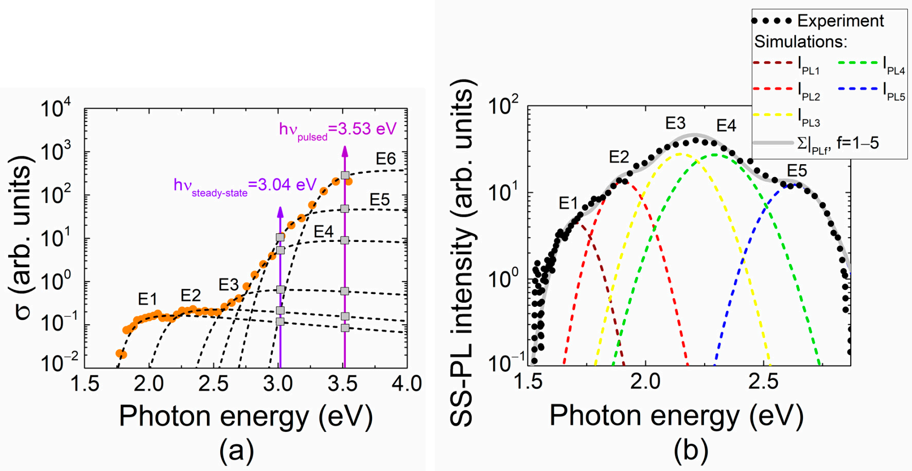
Photoluminescence excitation in our experiments was performed by UV (354 nm) and violet (408 nm) laser beams, as mentioned above, to separate the prevailing radiative recombination centers. The UV laser beam generates excess carriers through inter-band electron transitions, which later recombine through excitonic annihilation and radiative processes via deep electronic states ascribed to various defects. Together with inter-band processes, the excess carriers can be generated by photo-ionization of defects, leading to a step-like spectrum of absorption. The pulsed photo-ionization spectra (PPIS) recorded at room temperature in MOCVD GaN are illustrated in Figure 1a. Several carrier photoactivation centers (up to six traps for photon energies in the range of 1.0–3.3 eV) are inherent to MOCVD GaN materials. Separation of the PPI spectral steps was accomplished by controlling whether the same step appeared in different samples. Non-resonant excitation was implemented using fixed-wavelength light (354 and 408 nm) illumination with relative efficiency (determined by relative absorption coefficients and denoted in Figure 1a by square points) attributed to various defects. An absorption coefficient αd (hν) = σd (hν)nd related to a definite trap also depends on filling of its levels nd .
Figure 1a shows the σd (hν) spectrum illustrating αd (hν) with normalized nd distribution inherent for MOCVD GaN materials. It can be deduced from Figure 1 that excess carriers excited by UV laser are capable of inducing photo-luminescence from all the traps (highlighted as the spectral steps) including exciton annihilation, followed by phonon replicas, while the laser diode radiation at 408 nm wavelength affords ionization of the centers with activation energy less than that of the E5 trap. The origin of traps, tentatively identified by coinciding peak values of activation energy referenced in literature, is denoted in Table 1.

Figure 1. (a) The photo-activation centers (E1–E6) resolved from the photo-ionization spectral steps, measured on MOCVD GaN (scattered circles-data) and simulated using Kopylov–Pikhtin approach (Equation (1))-dashed lines. These traps were tentatively identified using the activation energy values taken from the literature referenced. The peak values of spectral bands were adjusted by varying the trap concentration parameters. Arrows denote the photon energy for fixed wavelength excitation of photoluminescence employed in these experiments. The gray rectangles indicate a relative efficiency of PL excitation by intersection of photon energy with spectral shapes of the identified photo-ionization centers. (b) PL spectrum (black circle symbols) recorded on MOCVD GaN material at room temperature using the multi-functional WITEC system Alpha 300 in confocal microscopy mode. This measured spectrum was fitted (gray solid line) using the van Roosbroeck– Shockley model (Equation (2)). This simulated gray solid line represents a resultant PL spectrum of simultaneous action of photoactive centers revealed by pulsed photo-ionization spectroscopy (PPIS) techniques. The contribution of each center (dashed lines) was simulated using parameters extracted from PPIS analysis. Fitting of the experimental PL spectrum (scattered circles) by a simulated resultant PL spectrum (solid gray curve) was implemented by slightly adjusting the contribution of various centers (dashed lines). The latter procedure was performed by varying the peak amplitudes (related to concentrations of definite centers).

Table 1. Activation energy estimated by fitting PPI spectral steps recorded on MOCVD GaN and associated with different defects. Origin of these defects was identified using experimental activation energy values and theoretical parameters estimated based on configuration diagram models referenced in literature.
A predicted PL spectrum in MOCVD GaN (simulated using photo-ionization spectroscopy data) is illustrated in Figure 1b. The red-shifted (relative to photo-ionizationspectral peaks) bands of yellow-green luminescence (YC-PL), composed of the radiativerecombination through E-E, traps, and blue (B-PL) luminescence are in line with ourexperimental observations in photo-ionization and photoluminescence spectra. Here, theYC-PL band is determined by the radiative recombination through E1-E, traps, while B-Plappears due to E; traps. The additional recombination channel, observed as a violet plVPL) band (within spectra illustrated in Figure 2d-f), peaked at 3.2-3.3 eV, and it has beertraditionally (Ref. (42) attributed to the donor-acceptor pair recombination.

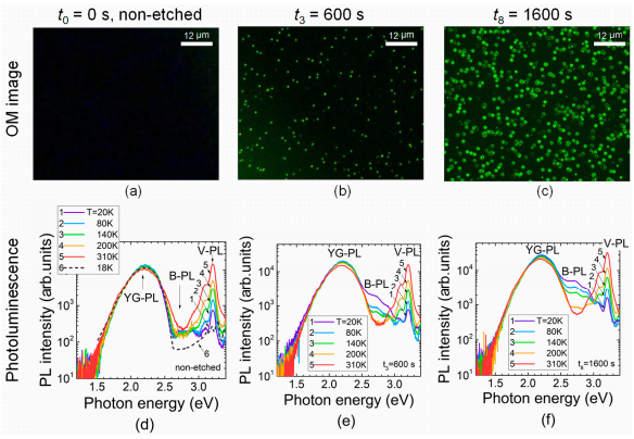
Figure 2. (a-c) Evolution of optical microscopy (OM) images dependent on etching exposure.d-f) PL spectra measured at different sample temperatures and dependent on etching exposureduration (f) when an H3PO4 temperature of 150 °C was kept over etching procedures. A sketchcurve 6) of the PL spectrum typical for the MOCVD grown GaN is taken from Ref. (43] and plottedin Figure (d) as a dashed curve for comparison of inherent spectral structures.
3. Correlation of PL Spectra with Etch-Pit Profiling Scans in MOCVD GaN Layers
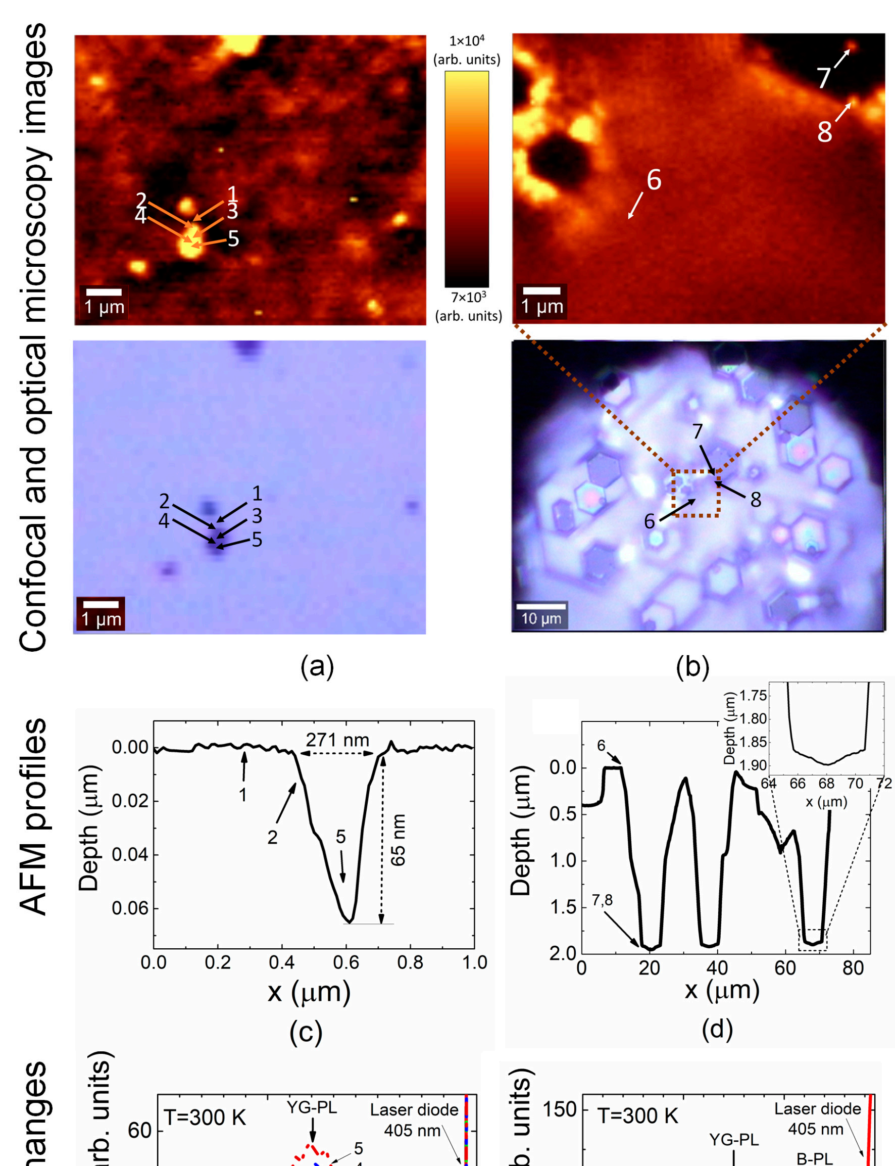
PL spectra in the etched samples were examined under pulsed UV excitation in awide temperature range of 20-300 K. Evolution of these spectra as a function of 150 °(H,PO, etching exposure is illustrated in Figure 2. The changes in spectrum structure and PL intensity were mainly obtained within blue PL bands when analyzing the sample.covering the entire etching exposure range. Therefore, spectra ascribed to the initial andfinal stages of etch processing and the intermediate regime of 600 s exposure are illustratecin Figure 2. No surface pits could be resolved in the pristine sample (to = 0 s). Etchingpits appeared after even a short etching duration (tg = 600 s). Either cone- (t3) or hexagon(tg = 1600 s)-shaped pits (Figures 2 and 3c,d) appeared due to different rates of lateraland depth removal of material. The lateral dimensions of etching pits clearly increasedwith etching exposure when comparing the spatial extension of the etch-pit-profiles aftert; = 600 s and ts = 1600 s (Figure 3) exposures.
4.Discussion
The relations between photo-ionization (PI) and photo-luminescence (PL) spectra enable the prediction of a structure of Stokes-shifted PL bands on the basis of photoexcitation spectroscopy. Additionally, analysis of these correlations could serve for more reliable identification of the origin of the photoactive centers and their roles in the formation of PL bands.
The presented characteristics of our experiments imply that the YG-PL band, peaking at 2.2 eV, is composed of PL processes ascribed to several E1–E4 photoactive centers, namely Ga vacancies (VGa) and charged carbon impurities localized on N sites (CN −). This YG-PL band has a more sophisticated origin (relative to that ascribed to a single type defect), as deduced from the correlation of photo-ionization and photo-luminescence spectra, compatible with comprehensive experimental results. The observed V-PL band, ascribed to radiative recombination through donor-acceptor pairs, can only be induced using UV excitation of excess carriers through inter-band transitions. The revealed B-PL in our experiments should be ascribed to point defect complexes decorating the cores of dislocations. This ascription is inferred from the appearance of the B-PL correlated with an etch-pit profile and the formation of a B-PL containing wide-PL bands at boundaries of deeply etched hexagonal valleys, as illustrated in Figure 3.


Figure 3. Correlation among confocal microscopy (of PL integrated within 450 to 720 nm spectralrange) and optical microscopy images (a,b), as well as atomic force microscopy (AFM) profiles(c,d) and PL spectral variations (e,f). The numbered localized etch-pits (a) and the intersection ofetched areas (b) obtained with enhanced spatial resolution are illustrated in top figures (a,b). Therelated optical images (bottom figures (a,b)) obtained in reflected light on the examined sample areas.lhe atomic force microscopy profiles scanned close to a single etch-pit (c) highlighted after shortetching exposure; and rather extended areas (d) of the intersecting etched surfaces, formed underong etching procedures. The shape of the dislocation-ascribed single etch-pit can be employed foridentification of dislocation type (as the edge dislocation ascribed etch pit illustrated in (c)). Thedeep etch-pits ascribed to either screw- or mixed type dislocations can be assumed by analyzingintersections of wide area etched hexagon valleys (d). The blue PL band spectral components appearonly (e,f) when the confocal microscopy probe is localized either close to the core (location 2 in(a,c,e)-assuming dimensions of space charge region Ro) of the single dislocation or steep planes ofhexagonal valleys ((b ,d,e), respectively). Numbers (1-8) denote locations nearby etch-pits where thePL spectra are recorded.
5.Summary
It has been found that red-shifted, relative to photo-ionization spectral peaks, bandsof yellow-green luminescence (YG-PL) and blue (B-PL) luminescence are observed under pulsed UV excitation. The cross-correlations of the photo-ionization and photoluminescence spectra, ascribed to the point photoactive centers, can be well simulated usingthe Kopylov-Pikhtin approach in the description of the absorption steps and vanRoosbroeckShockley relation to transform the photon-electron interaction cross-section data into photoemission spectra. It has been shown that this cross-correlation enables prediction of theStokes shifts between the outspread PPIS steps and the respective PL band peaks. Therecombination channel, ascribed to the violet PL band and peaking at 3.2-3.3 eV, corresponds to the donor-acceptor pair recombination. The additional B-PL band peaking at2.7-2.9 eV has been revealed in the etched samples. The combination of different excitationwavelengths enabled the estimation of the prevailing PL centers. Carbon-oxygen CyONcomplexes prevail when 354 nm of excitation can efficiently stimulate electronic transitionswithin C On defects, while 408 nm of illumination activates the Cy centers. The hydrogen complexes with carbon-originated point defects seem to be the non-homogeneouslydistributed blue luminescence centers, which decorate cores of dislocations. This B-Pl isweak in non-etched samples at elevated temperatures when excess carriers diffuse out ofdislocation cores, and B-PL light extraction is inefficient. The intensity of the latter B-PIband increases with sample cooling and etching exposure. Correlation of the B-PL bandintensity with dimensions of etching-pits implies the relations of these B-PL centers todislocations, where B-PL appears, and its peak amplitude increases with increased etchingduration (t). The transforms of the etch-pit shape and dimensions simultaneously manifestwith the increase in exposure. It has been inferred from the analysis of the evolution of Pl topography that the B-PL band appears when the excitation beam is localized at the bound.ary of the single etching-pit, ascribed to a single dislocation. The wide area and deepletched hexagon-shaped valleys appeared under prolonged etching exposures, followed bthe formation of broad spectral bands spreading out into the B-PL range. The revealed B-Pl could be ascribed to the point defect complexes decorating these cores of dislocations. Thisoutcome has been deduced from the appearance of the B-PL correlated with the etch-piprofiles and formation of B-PL-containing wide PL bands at boundaries of deeply etchedhexagonal valleys.
The evolution of the B-PL band with etching exposure has been explained by assuming local variations in PL light extraction efficiency when the area and geometry of cone or hexagon terrace boundaries are modified. The etching-pits appear due to different etching rates for horizontal rh and vertical rv removal of GaN material and based on scans of etch-pit dimensions dependent on acid temperature and etching exposure time t. It has been shown that the coefficient M~(rh t) 2/R0 for the total enhancement of B-PL intensity can be estimated using the ratio of light extraction areas M ≈ (π/R0)(rh t/2)2 when comparing these values in etched (~t 2 ) and non-etched (with radius R0 of dislocation core) samples. The etched GaN surfaces might also increase the efficiency of PL excitation (due to enhancement of the excited area), resulting in a greater number of excess carriers and radiative recombination photons within etched samples. A model of evolution of B-PL intensity with etching exposure has been approved.
搜索“华林科纳行业观察”小程序查看完整内容,或者加微信13358064333/18106288187。
下一篇: 超低损耗 Si3N4 的晶圆级加工