Abstract
Photonic integrated circuits (PICs) are devices fabricated on a planar wafer that allow light generation, processing, and detection. Photonic integration brings important advantages for scaling up the complexity and functionality of photonic systems and facilitates their mass deployment in areas where large volumes and compact solutions are needed, e.g., optical interconnects. Among the material platforms available, silicon nitride (Si3N4) displays excellent optical properties such as broadband transparency, moderately high refractive index, and relatively strong nonlinearities. Indeed, Si3N4 integrated waveguides display ultralow-loss (few decibels per meter), which enables efficient light processing and nonlinear optics. Moreover, Si3N4 is compatible with standard complementary metal oxide semiconductor (CMOS) processing techniques, which facilitates the manufacture scalability required by mass deployment of PICs. However, the selection of a single photonic platform sets limitations to the device functionalities due to the intrinsic properties of the material and the fundamental limitation of optical waveguiding. Multilayer integration of different platforms can overcome the limitations encountered in single-platform PICs.
Silicon nitride was initially used as an insulation layer in CMOS processes, but it became successful in the photonic field thanks to its large transparency window (400-4000 nm) , the Kerr nonlinearities and the lack of two-photon absorption, which makes it ideal for nonlinear optics. Moreover, the possibility to be manufactured on planar Si wafers and the CMOS compatibility of the processes makes it a good candidate to substitute Si as a passive platform.
The transparency window of Si3N4 enabled applications in the very near IR, and visible spectrum, instrumental for biosensing, augmented reality and the current standards in data center interconnect, operating at 850 nm. This frequency range is less demanding in terms of film quality compared to the telecommunication range at 1550 nm (C-band) , but it is characterized by increased scattering loss due to the shorter wavelength.
In the telecom bands (1300-1600 nm), the moderate index contrast between 3Chapter 1. Introduction Si3N4 and SiO2 reduces the scattering loss due to sidewall roughness compared to SOI waveguides. Indeed, loss below 0.1dB/m can be achieved in ultrathin waveguides with low confinement . However, the low confinement geometry, requires large bending radii, in the order of mm, which drastically decreases the integration density. Moreover, a single core waveguide cannot be dispersion engineered to attain anomalous dispersion, limiting the possibility to exploit the Kerr nonlinearities of the core material. For this reason, thicker Si3N4 layers were deposited, with a great effort to bypass the crack generated by the tensile stress of the material. Different methods were developed and an overview is reported in Section 3.2.
Integrated photonic devices are capable of guiding light in narrow waveguides thanks to the index contrast between the core and cladding materials. The crosssectional geometry of the core can be engineered to tailor its properties, e.g., the number of supported modes and the dispersion. However, the performance of real waveguides can significantly differ from the simulation due to fabrication imperfections. In this chapter, we describe how a waveguide can be engineered to fulfill the specification required by the intended application and how the fabrication can influence the outcome.
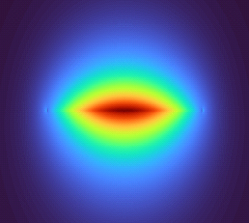
The polarization of the mode is defined by which field is oriented in the x transversal direction (ˆx), following the axis in Fig. 2.1. When the electric field is parallel to ˆx, the mode has transverse electric (TE) polarization, while when the magnetic field is parallel to ˆx the mode has transfer magnetic (TM) polarization. It should be noted that pure polarization states are not possible in optical waveguides. Indeed, in the vector wave equation, the inhomogeneity due to the material interfaces couples the transversal and longitudinal components of the field. However, the components in the other directions are negligible compared to the component in ˆx, as shown in Fig. 2.2.


Figure 2.1: Simulated fundamental TE modes calculated at a wavelength of 1550 nm for core dimensions a) 50 × 5000 nm2 and b) 800 × 1800 nm2

Figure 2.2: Components of the electrical field for the fundamental TE mode of the waveguide in Fig. 2.1b. The field is normalized so that the maximum of the field intensity |E| 2 is 1.
The simulation of optical modes requires an accurate evaluation of the material parameters, namely the refractive index and the film thickness. The measurement of the refractive index is based on the refraction of light at an interface, as described by Snell’s law. The direct measurement of the angle of refraction is still used in handheld refractometers to evaluate the sugar concentration of aqueous solution, a common measurement in winemaking. However, these direct measurements rely on the absolute intensity of the light, which is dependent on material imperfections. For this reason, a more sophisticated technique called ellipsometry is used in the CMOS industry.
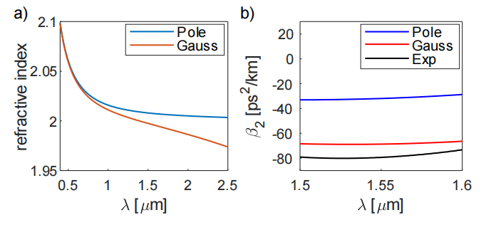
In our cleanroom, we inspect the Si3N4 deposition (see Chap. 3) with a spectroscopic ellipsometer1 in the wavelength range of 210 to 2500 nm. The blue line in Fig. 2.4a represents the refractive index of Si3N4 evaluated from the data collected with the offset-pole correction. This index was used to simulate the GVD of a bent waveguide reported in Fig. 2.4b (blue). If we compare this data to the experimental GVD calculated from the response of a ring resonator (black), we can notice a great discrepancy between the values. For this reason, we apply a different correction to the model by substituting the pole with multiple Gaussian oscillators in the mid-IR region of the spectrum (>5µm). These Gaussian oscillators were determined by a broadband ellipsometry measurement (210-30000 nm) done at J.A. Woollaam and are added to the index model as constant. This correction results in the red curves in Fig. 2.4. It is clear that they introduce a significant difference in the refractive index, especially in the most interesting portion of the spectrum for us, i.e., at 1550 nm. This provides more accurate simulation results, as we can see in Fig. 2.4b. A discrepancy of ∼10 ps2/km is still present, suggesting that more investigations are needed. A possible effect is the stress introduced by the deposition of the cladding, which can affect the index of the layers below, as reported in ref. .

Figure 2.4: Index models for Si3N4: a) comparison between the index calculated using a pole in the mid-IR and a series of experimentally calculated Gaussian oscillators. b) Comparison between the simulated GVD obtained with the two index models and the experimental value obtained from one of the devices in Paper E.
搜索“华林科纳行业观察”小程序查看完整内容,或者加微信13358064333/18106288187。