Photonic integrated circuits have the potential to pervade into multiple applications traditionally limited to bulk optics. Of particular interest for new applications are ferroelectrics such as Lithium Niobate, which exhibit a large Pockels effect, but are difficult to process via dry etching. Here we demonstrate that diamond-like carbon (DLC) is a superior material for the manufacturing of photonic integrated circuits based on ferroelectrics, specifically LiNbO3. Using DLC as a hard mask, we demonstrate the fabrication of deeply etched, tightly confining, low loss waveguides with losses as low as 4 dB/m. In contrast to widely employed ridge waveguides, this approach benefits from a more than one order of magnitude higher area integration density while maintaining efficient electro-optical modulation, low loss, and offering a route for efficient optical fiber interfaces. As a proof of concept, we demonstrate a III-V/LiNbO3 based laser with sub-kHz intrinsic linewidth and tuning rate of 0.7 PHz/s with excellent linearity and CMOS-compatible driving voltage. We also demonstrated a MZM modulator with a 1.73 cm length and a halfwave voltage of 1.94 V.
Photonic integrated circuits (PICs) based on silicon (Si) have transitioned from academic research to use in data centers over the past two decades. In the recent wave of development, silicon nitride—initially motivated by its nonlinear properties for microcomb generation — has emerged as an integrated photonics platform in itself, offering low loss at the dB-meter level, nonlinear operation, high power handling capability, a wide optical transparency window and space compatibility. It has allowed novel capabilities including chip-scale optical frequency comb sources5 , traveling-wave optical parametric amplifiers , Erbium waveguide amplifiers , integrated lasers that operate in the visible and near UV spectral range , and is challenging the best bulk legacy lasers in phase noise and tuning. The commercial availability of lithium niobate on insulator (LNOI)—and ferroelectric thin film materials on insulator in general—can extend the functionality further by offering one of the highest Pockels coefficients, required to realize volt level high-speed modulators, electro-optical frequency combs16, photonic switching networks, delay lines, on-chip broadband spectrometers and lasers. Periodic poling of thin film-based LiNbO3 ridge waveguides has allowed on-chip frequency doublers, squeezed light sources and optical parametric oscillators. LiNbO3 also features large second-order nonlinear susceptibility for optical frequency conversion and piezoelectric coefficient enabling advanced on-chip acousto-optics. Integrated photonic circuits critically rely on achieving wafer-scale manufacturing, which also exhibits low loss and attains lithographic precision and reproducibility. A critical manufacturing step is the etching process, which transfers the lithographic pattern into the photonic device layer. While for currently employed foundry-compatible photonic material platforms, in particular, silicon or silicon nitride, mature processing is available, the latter cannot be readily extended to the rapidly emerging platforms based on ferroelectric materials, such as lithium niobate on insulator. Direct etching of lithium niobate is usually based on argon ion bombardment, which is a strong physical process that cannot achieve a high etch selectivity between lithium niobate and common hard mask materials, such as SiO2 and a-Si (see comparison of different dry etching methods in Supplementary Fig. 2). As a result, state of the art in LiNbO3 integrated photonics technology are shallow ridge waveguides with close to unity ridge to slab ratios and strongly slanted sidewalls (≈60∘ ). The thick slab entails strong limitations in terms of waveguide bending radius as well as requiring more challenging process control due to the partial etch. This complicates efforts to establish and qualify process design kits for LiNbO3 photonic integrated waveguide platforms. Metallic masks, such as chromium, feature high etch selectivity but are polycrystalline with rough sidewalls and optically absorbent etch product redeposition. Heterogeneous integration of LiNbO3 with silicon or silicon nitride integrated photonic circuits is another approach. Such hybrid waveguides have been successfully achieved, with excellent low loss performance, yet exhibit additional complexity due to the use of wafer bonding onto pre-fabricated substrates, and requiring tapers for mitigating losses from transitioning into and out of the bonded areas. Hence a LiNbO3 photonic integrated circuit platform featuring ultra-low loss fully etched strip waveguides with vertical sidewalls, already well established and successfully commercially employed for silicon and silicon nitride, would be highly desirable. Here we overcome this challenge by introducing DLC, diamond-like-carbon, as a hard mask process, and demonstrate LiNbO3 strip waveguide based photonic integrated circuits with high yield, ultra-low loss (<4 dB/m) that benefit from the 10- fold higher area density that previous ridge, i.e., partially etched, approaches.


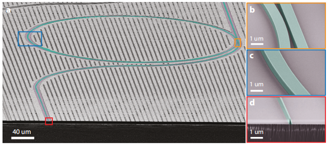
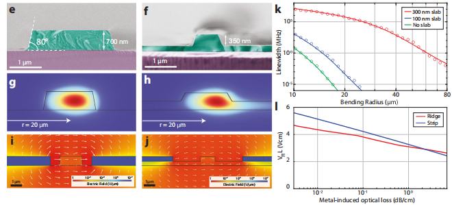
Fig. 1 | Tightly confining lithium niobate photonic integrated circuit platform. a Scanning electron micrograph (SEM) of a LiNbO3-based photonic integrated circuit with high resolution insets of microring coupling section ((b, orange), curved waveguide (c, blue), and inverse taper for fiber coupling (d, red)). e SEM of a fully etched optical waveguide with cross section 2 μm × 0.7 μm.f SEM of a partially etched ridge waveguide 1.5 μm × 0.6 μm, 350 nm etch depth and 250 nm LiNbO3 slab. g, h Optical mode field distribution of curved waveguides corresponding to (e, f) with 20 μm bend radius. i, j Electrical field distribution in log-scale for slab and ridge waveguides with electrode spacing 0.75 μm and 2.5 μm, which are selected to feature equal metal-induced optical losses. k FEM simulations of LN waveguide bending loss for different slab heights and waveguide cross-section 2 μm × 0.6 μm. l FEM simulation of the voltage-length product of electro-optical modulation for strip and ridge waveguides as a function of metal-induced waveguide loss.

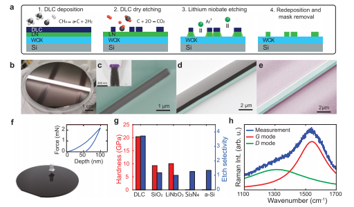
Fig. 2 | Fabrication process based on diamond-like carbon (DLC) hardmask. a Process flow of the LNOI waveguide fabrication including diamond-like carbon (DLC) hard mask deposition via plasma enhanced chemical vapor deposition (PECVD) from methane precursor, DLC dry etching via oxygen plasma, lithium niobate etching via argon ion beam etching (IBE), followed by redeposition and mask removal. LiNbO3 is illustrated in green, SiO2 in light blue, DLC in dark blue and Si in gray. b Photo of a deposited DLC film on the silicon wafer. SEM images of the taper pattern and the cross section with 250 nm width after DLC dry etching (c) DLC mask and the LiNbO3 waveguide after redeposition cleaning (d) and the LN waveguide with 0.7 μm height and 2 μm width after mask removal (e). In the SEM images, the LiNbO3 is colored in green, DLC in black, Si3N4 in purple and SiO2 in light purple. f The schematic and the result of indentation hardness measurement for DLC. g Hardness and etching selectivity chart for different materials. h Raman spectrum and fitting result for DLC film.
Fabrication process with DLC hard mask Figure 2a depicts the schematic process flow of our low-loss LiNbO3 strip waveguide fabrication. We start the fabrication using commercially available thin film lithium niobate on insulator wafer (NanoLN) with X-cut(600 nm) or Z-cut(700 nm) thick LiNbO3 layer, 4.7 μm buried oxide (thermally grown) on a 525 μm thick Si substrate. The salient feature of our fabrication process is the use of a 300 nm thick DLC film, which is grown via PECVD from a methane precursor, as a hard mask material for the physical ion beam etching process. The diamond indentation hardness of the as-deposited DLC film is 19–23 MPa (see Fig. 2f and Supplementary Fig. 1), which is up to two times harder than SiO2 and LiNbO3. The chemical composition of the film is measured via Raman spectroscopy38 (see Fig. 2h). Analyzing the two C-C stretch modes (D,G) at 1312.4 cm−1 and 1541.0 cm−1 , we find that our film contains up to 5% sp3-hybridized C-atoms and a large hydrogen content, which classifies the material as amorphous diamond-like carbon (aC:H), typical of PECVD deposition using methane precursor. We have carefully optimized the process to facilitate wafer-scale uniform growth of DLC for minimal stress and particle contamination, which is pivotal to the manufacture of photonic integrated waveguide structures. The optical waveguide pattern is structured by DUV stepper photolithography (248 nm) and first transferred into a Si3N4 mask layer using standard fluoride-chemistry-based plasma etching. This intermediate mask has excellent resistance to oxygen plasma etching, which we use to transfer the waveguide pattern into the DLC hard mask (see Fig. 2c). With optimized argon ion beam etching (IBE), the etching selectivity between LN and DLC is up to ×3, which enables deep etching and steep sidewalls. Figure 1e contains an SEM cross section of the fully etched LiNbO3 strip waveguide with waveguide base width of 3.3 μm and height of 0.7 μm featuring an 80° sidewall angle. Currently employed soft SiO2-based masks are limited to an etch selectivity of ×1 in comparison. The film hardness directly correlates with the material etching rate in IBE, which is plotted as the etch selectivity compared to LiNbO3 in Fig. 2g. Remarkably, our film hardness of 20 GPa lies at the lower limit of the attainable hardness range of DLC thin films. We remove the rough LiNbO3 redeposition on the waveguide sidewall using SC-1 solution (NH4OH: H2O2: H2O=1:1:5) (see Fig. 2d) and the residual DLC mask (see Fig. 2d) using oxygen plasma to reveal the waveguide core (see Fig. 2e). The oxygen plasma from a photoresist ashing tool is sufficient to completely remove the DLC without leaving any residues and this solution also causes no damage to the lithium niobate. Next, we fabricate the electrodes via a DUV-stepper lithography-based lift-off process for which we deposit 5 nm titanium adhesion layer and a 400 nm gold layer via electron-beam evaporation. Finally, the wafer is separated into chips via deep dry etching followed by backside grinding to obtain clean, vertical and smooth facets without a silicon pedestal for efficient waveguide edge coupling.
Discussion
In summary, we developed a platform for high-density lithium niobate on insulator photonic integrated circuits based on a deeply etched strip waveguide with tight optical confinement based on a micro structuring process featuring amorphous carbon films (DLC) as etch mask (see performance comparison of integrated lithium-niobatebased platforms in Supplementary Table 1). Our process is readily applied for a wide variety of photonic materials that are resistant to oxygen plasma etching, which includes silicon, silicon dioxide, silicon nitride and notably also ferroelectric oxides beyond LiNbO3 such as BaTiO3 or LiTaO3. At similar loss levels compared to LiNbO3-based ridge waveguides, our fully etched geometry affords four times smaller minimum bend radius, which corresponds to a potential increase of photonic component density by a factor of 16 without sacrificing significant electro-optical modulation efficiency, which is advantageous for applications in classical photonic and quantum computing with large switching fabrics or photonic networks. In a similar manner, the increased optical confinement and small bend radii can greatly benefit other electro-optical quantum technologies such as quantum coherent microwave to optical converters. Electro-optic materials can enable lasers with flat actuation bandwidth and very fast optical tuning up to multi-MHz bandwidth. Such a system is an attractive candidate for applications in coherent (FMCW) laser ranging and critically enables to reduce the voltage driving to CMOS level while achieving GHz tuning range, excellent linearity, no measurable hysteresis, and low laser phase noise.
搜索“华林科纳行业观察”小程序查看完整内容,或者加微信13358064333/18106288187。
下一篇: 光互连CPU技术