Abstract
In the CMOS process, there are 4 materials, silicon nitride (Si3N4), silicon oxynitride (SiOxNy), silicon dioxide (SiO2), and silicon (Si) that can be used as an optical waveguide. If silicon is not used, then the waveguide should be made with the remaining 3 materials. Among the methods that can inject light into those optical waveguides, the only possible method is to use a prism. It is demonstrated that an optical network chip can be realized by our three technologies and the cavity-type waveguide made out of silicon nitride and silicon dioxide.
The average propagation loss transmitted through the cavity-type waveguide, which was designed to minimize roughness on the waveguide side walls, was measured 0.258 dB/cm. Except for the reflection loss at the prism, the net coupling loss from VCSEL to the waveguide was measured 0.855 dB. The packaged size of VCSEL or photodiode has an area of 0.4 mm2 and a height of 0.64 mm, which can be attached to the prism. The area for optical devices to be integrated on a 8 core CPU chip is much smaller, <30 mm2 , than the available area, 174 mm2 .
The prism used for injecting light into the waveguide can also be used as the optimal WDM filter in which two thin films with different refractive indices are alternately stacked on the bottom side. Theoretical calculations have proved the performance of a WDM filter. If anti-reflection films were coated on the two surfaces of the prism with materials, TiO2 and Ta2O5, then the reflection loss at the prism was calculated to decrease from 2.75 dB to 1.11 dB for polyimide adhesive and from 2.73 dB to 0.52 dB for optical glue.
I. INTRODUCTION
A number of optical communication-based network architectures for CPU application have been proposed, but they have not reached the stage of experimental integration and testing on actual chips. Recently the lower complexities of photonic processor chips and switching chips integrated with electronic devices have been demonstrated experimentally.
The difficulties for implementing the proposed network architectures can be listed as follows. The first is the disadvantage of using SOI wafers. Wafers used in CPU and memory chip production are ordinary bulk silicon. The fact that electronic devices and optical devices can be manufactured with the same CMOS process on the same wafer, which motivated the research of silicon photonics, did not have many benefits in reality. When using a silicon optical waveguide, the optical waveguide and the optical device should be arranged in the same silicon layer as the gates of the CPU. This is disadvantageous not only in increasing the gate density of the CPU, but also in designing metal layers of CPU or DRAM. Contrary to the motives, for most proposed architectures, it is assumed that optical devices and CPU were manufactured on different wafers and bonded in a 3D package structure .
Second, the transmission loss of the silicon optical waveguide is large. Silicon has a high refractive index (n = 3.45), which is advantageous in making the size of the optical waveguide as small as possible, but disadvantageous in designing a low transmission loss of waveguide. Although ATAC assumed a loss of 0.3 dB/cm, the minimum value reported in the paper is 1~2 dB/cm, but in a typical CMOS process, it is measured to be larger than 2 dB/cm.
Third, the yield and performance of optical modulators, detectors, and ring resonators are far below implementation on a network-on-chip. For the network to function, the failure rate of each device needs to be lower than the redundant device rate (generally 10 %). The average yield has to be over 90 %. When manufacturing modulators and detectors by epitaxial growth of Ge materials on silicon wafers, it is difficult to obtain a uniform yield by the necessary ratio. Particularly, it becomes nearly impossible when it is accompanied by fabrication-attributed statistical errors such as the resonance wavelength of the ring resonator. In this case, micro-heaters need to be attached locally and heated for wavelength tuning. Heating 500,000~1.1 million resonators contained in a network chip removes the advantage of optical signals. Furthermore, it is assumed that the insertion loss of optical modulators is approximately 1 dB for most proposed architectures, but the reported insertion loss is about 3~6 dB, which is a significant difference.
The fourth is the light source. An on-chip laser implemented by joining an InP wafer to a silicon wafer suffers yield problems similar to a Ge-based optical device. Most architectures are presumed to use external light sources, but it is difficult to integrate hundreds to thousands of lasers in the alignment of optical fiber arrays with optical waveguide arrays on a chip. It is also difficult to secure space to attach them on the side of the chip when considering the cross-sectional area of the optical fibers. The coupling loss measured when aligning one optical fiber to a silicon optical waveguide is reported to be a minimum of 1 ~ 2 dB, but it is only accomplished by modifying or adding a special structure at the inlet of the optical waveguide. In general, coupling loss is measured to be 3~6 dB or more.
II. THREE TECHNOLOGIES
First, an adhesive technology that is transparent, satisfies the refractive index matching condition, maintains its adhesive strength at 200-400 °C, and is not affected by solvents used in the CMOS cleansing process such as BOE, isopropanol, acetone, etc. needs to be achieved. There are no commercial adhesives that are transparent with a refractive index greater than 1.6 for the wavelength, 850-1550 nm. Adhesives that maintain their strength in cleansing solvents and at 400 °C have not been reported in any papers. Therefore, it is necessary to develop a technology that can bond a prism to the surface of an optical waveguide without using a commercial adhesive.
Second, a microlens that can produce collimated light under the conditions of Fig. 1 needs to be achieved. Microlenses consisting of quartz and silicon materials are commercially available, but their refractive indices are not suitable for the current purpose. VCSELs fabricated with such microlenses in references are not expected to be available commercially in the near future. Third, a special package technology for VCSEL and PD needs to be achieved. The current commercial package has a hermetically sealed structure that gets filled with nitrogen gas, maintaining a specific distance between the laser light exit and the lens. This type of packaging is overly bulky, and dozens to hundreds of VCSELs and PDs cannot be integrated on the CPU chip. We have developed an adhesive technology, a stand-alone polyimide microlens, and a packaging technology that satisfies the requirements.

Fig. 1. Conceptual diagram of optical coupling on SiON optical waveguide.
Fig. 2 (a) is a micrograph of a GaP prism bonded to the surface of a SiON optical waveguide and (b) is an enlarged photograph of the sideview. Thermo-set polyimide and our specially developed procedure were used for bonding. The adhesion characteristics between the prism and wafer are shown in Table I. It had a transmissivity of over 99 % at the thickness of 2 μm required for adhesion, and the refractive index was measured to be up to 1.72 depending on the heat treatment conditions applied to the polyimide. When force was applied from the side to observe the adhesion strength, the prism broke more times than it fell off.
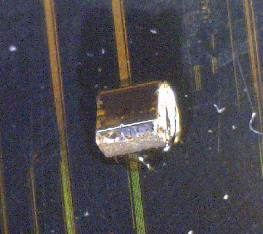
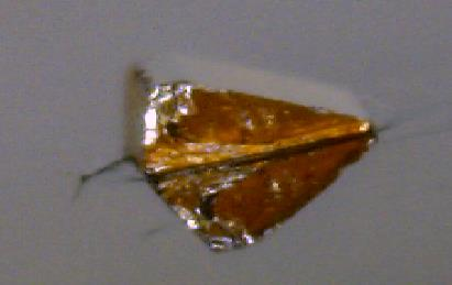
Fig. 2. Images of prism bonded to SiON optical waveguide, (a) top view, (b) sideview.
The radiation angle of VCSEL in the air is typically in the range of 20~40°. The microlens must have the right value of refractive index to collimate light emitted by the median value of 30°. Fig. 3 shows a scanning electron microscope (SEM) image of the polyimide microlens array (a) and an enlarged image (b) of one. The diameter of the microlens is 30 μm. The properties of polyimide microlens are shown in Table II. As far as we have studied, this is the first report of a stand-alone polyimide microlens which was fabricated and imidized without VCSEL.
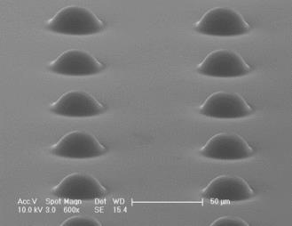
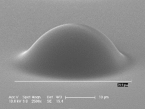
Fig. 3. SEM images of microlens, (a) array, (b) single.
After attaching the microlens to the 25 Gbps VCSEL chip, the shape of the output light was observed as shown in Fig. 4. The picture was taken by placing an infrared card 7 cm vertically from the VCSEL. Since the distance from the VCSEL to the optical waveguide is <1 mm, the collimated light proves a sufficient performance of the lens.
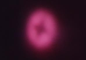

Fig. 4. Output light images of VCSEL before and after microlens attachment, (a) before, (b) after.
III. MODELING WDM FILTER AND AR-COATING
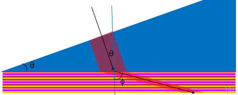
A WDM filter with a verified performance among the commercially available products is the thin film filter in which two thin films with different refractive indices are alternately stacked. Fig. 5 (a) shows the schematic diagram of four optical wavelengths transmitted through a single optical waveguide by coating WDM thin film filters on the bottom sides of the prisms. For example, λ3 passes through the prism coated with the filter of the corresponding wavelength and enters into the waveguide, and it is reflected off the bottom sides of the prisms coated with other wavelength filters and proceeds along the waveguide and is emitted from the prism of the corresponding wavelength. Fig. 5 (b) graphically shows the structure of a WDM filter and the light path.

(a)
(b)
Fig. 5. 4-channel WDM, (a) light input and output scheme, (b) thin film filter and light path.
IV.CONCLUSION
Universities and corporations have proposed various network architectures with optical communication technology, but they have not reached a status of experimentally integrating and testing them on actual chips. The difficulties can be attributed in large part to the property of silicon used as the optical waveguide.
In the CMOS process, there are 4 materials, silicon nitride (Si3N4), silicon oxynitride (SiOxNy), silicon dioxide (SiO2), and silicon (Si) that can be used as an optical waveguide. If silicon is not used, then the waveguide should be made with the remaining 3 materials. Among the methods that can inject light into those optical waveguides, the only possible method is to use a prism. It is demonstrated that the difficulties can be overcome by our three technologies and the cavity-type waveguide made out of silicon nitride and silicon dioxide.
The average propagation loss transmitted through the cavitytype waveguide, which was designed to minimize roughness on the waveguide side walls, was measured 0.258 dB/cm. Except for the reflection loss at the prism, the net coupling loss from VCSEL to the waveguide was measured 0.855 dB. The packaged size of VCSEL or photodiode has an area of 0.4 mm2 and a height of 0.64 mm, which can be attached to the prism. The area for optical devices to be integrated on a 8 core CPU chip is much smaller, <30 mm2 , than the available area, 174 mm2.
The prism used for injecting light into the waveguide can also be used as the optimal WDM filter in which two thin films with different refractive indices are alternately stacked on the bottom side. Theoretical calculations have proved the performance of a WDM filter. If anti-reflection films were coated on the two surfaces of the prism with materials, TiO2 and Ta2O5, then the reflection loss at the prism was calculated to decrease from 2.75 dB to 1.11 dB for polyimide adhesive and from 2.73 dB to 0.52 dB for optical glue.
搜索“华林科纳行业观察”小程序查看完整内容,或者加微信13358064333/18106288187。
上一篇: 高密度铌酸锂光子集成电路