Abstract
We report on an optimization procedure for depositing low-loss silicon nitride films at temperatures of 760 °C and 820 °C using low-pressure chemical vapor deposition. They were characterized in terms of quality and compositional proximity to stoichiometric silicon nitride. Films deposited at 760 °C showed a higher stoichiometry, with a silicon-to-nitrogen ratio of 0.744, when compared to the 820 °C film, which had a ratio of 0.77. We found the film deposited at the lower temperature had a smoother surface and exhibited lower optical losses. We investigated the impact of film stress on the refractive index of the film and found that removing the backside nitride from the wafer after deposition has a major effect on refractive index values. When using these films for integrated nonlinear and quantum applications, such as frequency conversion or soliton generation, knowledge of how the index changes with wafer and fabrication processing is critical for predicting the correct geometries, and the concomitant group velocities, needed to realize such quantum technologies.
INTRODUCTION
SILICON nitride has recently gained a lot of interest within the photonic device community as an attractive materials platform of choice for a wide range of applications including sensing, metrology, nonlinear optics, quantum information processing and telecommunications. Silicon and nitrogen are the two major elements of silicon nitride. Oxygen, hydrogen, and carbon are common impurities that affect the quality of silicon nitride films. Ideal silicon nitride films should have a stoichiometric composition where the silicon-to-nitrogen (Si/N) ratio is 0.75 and should be stable under high temperature and harsh chemical processing conditions. The refractive index of the stoichiometric silicon nitride films is slightly less than 2 and is a good indicator of stoichiometry, as a value greater than 2 implies a higher silicon content, which leads to higher optical losses. The material exhibits a diverse and versatile set of optical properties that span an extremely wide transparency band (e.g., UV to mid-IR). Having a refractive index slightly larger than silica and an extremely low coupling loss (<0.3 dB/facet) makes nitride an ideal choice for integrated quantum optics and can result in the removal of complexities in optical fiber. Control of the fabricated thickness of a silicon nitride waveguide layer allows for excellent dispersion engineering and more compact device footprints. The 5-eV bandgap energy of the material prevents two photon absorption effects and enables high-energy applications. This also helps to prevent or control unintended Raman or Brillouin scattering, which can cause deleterious effects on quantum noise measurements. The nonlinear index of silicon nitride is ten times higher than silica (∼2.0×10⁻¹⁹ m2/W) and allows for lower power requirements in chip-based optical processing and four-wave mixing generation. Furthermore, and the most cost-effective point, is that device fabrication techniques are CMOS compatible. Two common methods for depositing silicon are: low pressure chemical vapor deposition (LPCVD) and plasma enhanced chemical vapor deposition (PECVD). LPCVD-grown nitride has far superior film quality when compared to PECVD-grown films. High operating temperatures, between 750°C and 850°C, with low deposition pressures, between 0.2 Torr and 2 Torr, are the reasons why film quality is better; under these thermodynamic conditions, impurities and non-stoichiometry have a harder time incorporating within the film and is the reason they have ultra-low optical losses and high nonlinear indices. A main disadvantage of LPCVD systems is the use of toxic, explosive, or corrosive gaseous reactants. However, evolution of nanofabrication safety systems has greatly minimized such concerns. Typical values of the refractive index in these films vary from 1.95 to 2.1. LPCVD process parameters can be optimized to achieve stoichiometric compositions but at a cost of having very large, greater than 1 GPa film stress, that leads to relaxation processes causing film crazing and cracks. Hence, understanding, tracking, and controlling film stress is critical when fabricating photonic devices. Film stress can be tuned and can vary from a few hundred MPa to GPa tensile, depending on the LPCVD deposition conditions such as gases flow ratios, temperature, and pressure.
DEPOSITION
In this work, we employed LPCVD as it offers a higher quality film of nitride with lower loss over PECVD due to less impurities (i.e., hydrogen bonds). The gases used for the deposition process are dichlorosilane (SiH2Cl2), also known as DCS, and ammonia (NH3). The ratio of DCS/NH3 will determine the film properties, specifically whether the film is silicon-rich or stoichiometric. Stoichiometric nitride films (ratio <1) exhibit less loss than the silicon rich films (ratio >1) . However, the stress is generally higher, which leads to film cracking for thicknesses greater than 300 nm. This can be detrimental for some applications in integrated quantum optics, which require thicknesses to be above 500 nm. As will be explained in the stress control section, stress must be controlled or eliminated in device fabrication. A design of experiment (DOE) of the deposition process is shown in Table I. The temperature and the pressure were fixed at 820 °C and 300 mTorr, respectively, while the DCS/NH3 gases ratio were varied from 0.1 to 3. These values were chosen based on prior reports . The process was then repeated at 760 °C. Films with thicknesses of 200 nm and 500 nm were deposited on both bare silicon wafers and silicon wafers with a 5 µm thermal oxide isolation layer. Better refractive index fits can be achieved for depositions on bare silicon while the actual device fabrication will take place on wafers with thick oxide isolation layers. For film stress studies, the film thicknesses were 500 nm and 1000 nm, and both deposited on bare silicon and thick oxide isolation layers.
Film Loss Measurement (Metricon)
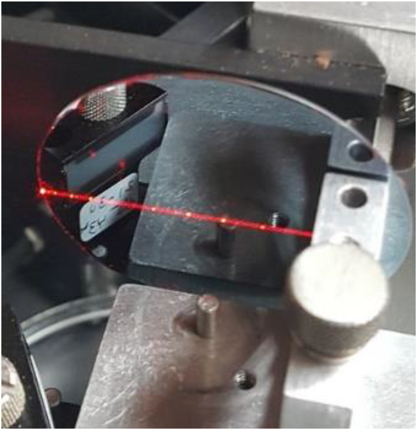
The Metricon Model 2010/M was used to evaluate the film loss. It utilizes a surface-mounted prism coupling technique to measure both the thickness and refractive index. Specifically, a prism was pushed against the wafer surface to couple the light through the film at the desired wavelength as shown in Fig. 1. The decaying of the coupled light during its propagation across the wafer provides an estimate of the bulk material loss. The 2010/M’s loss measurement option works over the range from 15 dB/cm to ≈ 0.1 dB/cm. Loss measurement near the lower limit of the tool may require further analysis with alternate methods to obtain the true values. Two nitride samples with a thickness of ∼ 380 nm (deposited at 760 °C and 820 °C respectively) were measured at 632.8, 983, 1312, and 1550 nm wavelengths.

Fig. 1. Metricon measurement setup and the coupling light at 632 nm wavelength is propagating across the wafer which is used to estimate the bulk material loss (the white shining spots are scattered light due to particles in the light path).
FILMS STRESS MEASUREMENTS AND STRESS CONTROL
Stress Measurements
A film stress measurement (FSM 900TC) tool was used to quantify the film stress at room temperature. This measurement allows one to obtain the wafer bow height and can measure wafer’s ranging from 2 to 8-inch. The stress values were evaluated based on the wafer bow pre- and post-nitride-backsideremoval scan). Backside nitride removal was achieved by reactive ion etching (Vision 320 RIE). The process parameters used for removing the backside nitride films were 20 sccm CF4, 2 sccm O2, RF power of 100 W, and a process pressure of 300 mTorr.
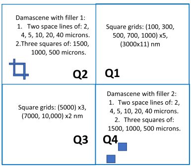
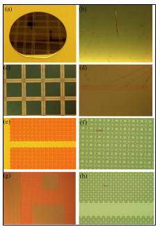
The most convenient and fastest way to prevent cracks from propagating in the film was to use a diamond tip to scribe lines vertically and horizontally (shown in Fig. 3(a) and (b)) to section off crack free areas during device fabrication. We patterned the oxide layer by using a photomask design (4 × 4 inches) as shown in Fig. 2 with 4 quarters (2 × 2 inches each). The quadrants Q1 and Q3 consist of square grids: 100, 300, 500, 700, 1000 of 5 rows each, 3000 of 10 rows in Q1 and 5000 of 3 rows, 7000, and 10000 of two rows each) in Q3. This photomask design will stop cracks from propagating and leave sufficient crack-free areas for device fabrication as shown in Fig. 3(c) and (d) . Two stress-release damascene designs were used in Q2 and Q4. Q2 forms an array of 10 × 10 of unit cells of dimension 5 mm × 5 mm with spacing of 1.5 mm used to put alignment marks for lithography processes. The Q2 unit cell is composed of slabs of filler design with two spacings in-between filler slabs of 2, 4, 5, 10, 20, and 40 microns to simulate different spacing widths which may be used for waveguides or other devices fabrication. On a top of these gradual spaced slabs are three empty squares of 500, 1000, 1500 µm2 with fillers around that would simulate device sizes like ring resonators. The Q2 filler consists of overlapped rectangles (Damascene #1 design), and each has a dimension of 2 × 20 microns as shown in Figs. 2,

Fig. 2. Stress control mask layout of the four quadrants (2 × 2 inches each). The quadrants Q1 and Q3 consist of square grids varying from 100 nm to 10 mm. The quadrants Q2 and Q4 have two different damascene designs that have been used to control the stress and stop the crack in the deposited thick nitride films. Details of the mask designs are explained in the stress control section.

Fig. 3. Fabricated and patterned structures: (a) Full 2-inch wafer scribed with diamond pen within a grid formation to stop the cracks and leave sufficient area for device fabrication. (b) Cracks were stopped from propagating across the wafer by the scribed lines. (c) Pre-patterned squares of 500 µm2 (Q1 design) on the oxide before the nitride deposition and it shows how the cracks are prevented from propagating. (d) Pre-patterned large square of 5 mm × 5 mm (Q3 design) used to prevent crack formation. (e) Q2 Damascene design #1 is shown with no cracks in the 40 µm spacing between two filler 1 slabs. (f) Zoomed in view of the Q2 filler 1 design. g) Q4 Damascene design #2 is shown with no cracks inside two squares of sizes 1 mm2 and 2 mm2 with filler 2 design filling around these squares. (h) Closer look into Q4 unit cell which shows that no cracks appear in the 40 µm spacing between two filler 2 slabs.
RESULTS AND DISCUSSIONS
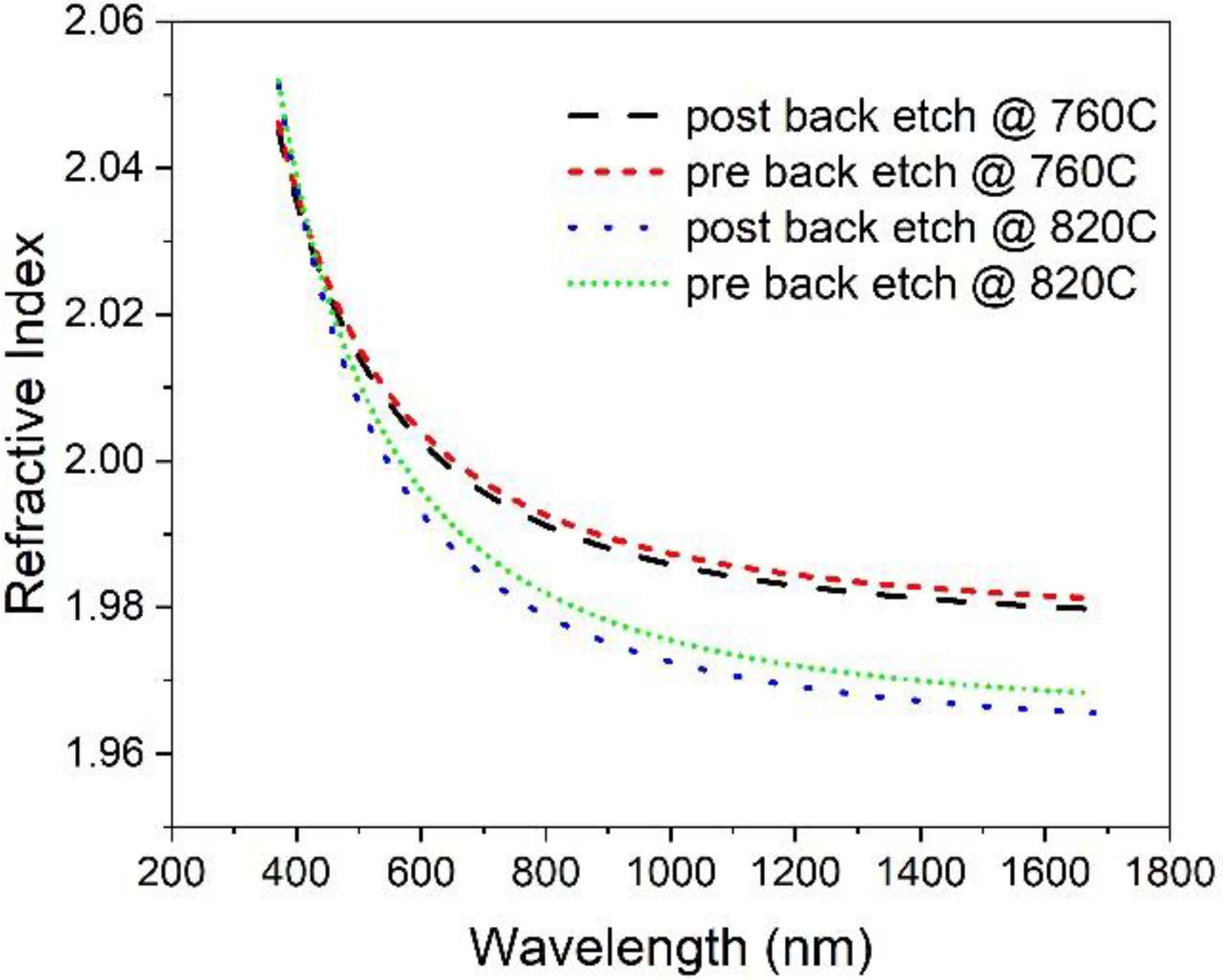
The deposition rates and refractive indices for films deposited at 760 °C and 820 °C were 2.49 nm/min and 1.985 (1.36 mean squared error (MSE)), and 5.5 nm/min and 1.9723 (1.48 MSE), respectively. The measurement wavelength was 1550 nm. Both values of the refractive indexes fall well within the range of stoichiometric silicon nitride (∼ ≤ 2.1, which depends on the wavelength, as shown in Fig. 4). Note that for some wavelengths, the value of the refractive index for the 760 °C film is lower than the 820 °C film. The deposition rate at 760 °C is lower than the value at 820 °C (< 50%). The lower deposition rate leads to smaller grains and good compacting resulting in higher film quality and lower optical losses. For both samples, the refractive index dependency on the wavelengths shows that it decreases as wavelength increases. Furthermore, it shows that for each film, the refractive index decreases when the stress increases after etching the backside nitride of the wafer. This phenomenon will be studied more and verified using multiple wafers with different substrates later in this section.

Fig. 4. Measured refractive index by ellipsometer for silicon nitride films of 500 nm thicknesses deposited at 760 °C and 820 °C, before and after the back side nitride removal. The graph shows a decrease in the refractive index value with the stress increase value after etching the back side nitride of the wafer.
CONCLUSION
Deposition methods and their parameters are critical in determining the overall quality and characteristics of fabricated silicon nitride films. Generally, LPCVD (>700 °C) is a preferred deposition method over PECVD (∼400 °C) as LPCVD leads to the production of higher quality films that contain less hydrogen bond impurities due to the higher temperatures. The ratio of NH3 and DCS gases used in the LPCVD process ultimately affects the final Si/N ratio of the fabricated film. Each recipe (i.e., gas flow ratio) results in a specific deposition rate, grain-packing, refractive index, and residual stress. In this study, we investigated different DCS/NH3 gas ratios and found an optimum ratio of 17.5 sccm/52 sccm = 0.3. Once identified, we performed further investigation into the quality of LPCVD deposited films at two different temperatures of 760 °C and 820 °C. Our results showed that films deposited at 760 °C exhibited a deposition rate (2.49 nm/min) that was 50% slower than those deposited at 820 °C (5.5 nm/min). Also, the results show that the refractive index values for both temperatures decrease with stress and increase after etching the nitride on the backside of the wafer. The stoichiometry of the films was evaluated using an 8-hour TMAH chemical etch at 80 °C. No etching was observed. Exact film composition was obtained through XPS and showed that the 720 °C film had a Si/N ratio of 0.744 while the film deposited at 820 °C was less stoichiometric with Si/N ratio of 0.771. The stress increase from backside nitride etching did not seem to have considerable impact on these ratios. The FTIR results showed peaks solely at 843 cm−1 for both films, before and after the backside etch, which indicated that only Si-N bonds were present. The AFM analysis illustrated that the average surface roughness of the films deposited at temperatures of 760 °C and 820 °C decreases by about 30% due to the stress increase (3.34 A° and 2.02 A°) and (3.56 A° and 2.38 A°), respectively. Different techniques, including some designs used for the damascene process, were evaluated for their ability to control and reduce stress. Lastly, we found that the refractive index of the film decreased with the increased stress due to etching the backside nitride. We found this increase of stress was consistent regardless of the substrate material under the nitride film (oxide or silicon) or the film thickness. In addition to having low-loss for single-photon operation, silicon nitride waveguides must have carefully controlled values of refractive index, as nonlinear optical processing of light depends upon second- and third-order dispersion and precise phase-matching conditions for integrated quantum optics. This work demonstrates that wafer and film processing may affect index values in a way that is unexpected resulting in unfavorable changes in the device performance, and so careful attention to fabrication steps are needed to ensure proper values of the refractive index are realized.
上一篇: 光互连CPU技术
下一篇: 硅衬底上的高度规模化 GaN 互补技术