Abstract— This article reports on the scaling of GaN complementary technology (CT) on a silicon substrate to push its performance limits for circuit-level applications. The highly scaled self-aligned (SA) p-channel FinFET (a fin width of 20 nm) achieved an ID,max of −300 mA/mm and an RON of 27 ·mm, a record for metal organic chemical vapor deposition (MOCVD)-grown III-nitride p-FETs. A systematic study on impact of fin width scaling and recess depth in these transistors was conducted. A new SA scaled n-channel p-GaN-gate FET (n-FET) process, compatible with the p-FinFET, demonstrated enhancement-mode (E-mode) n-FETs (LG = 200 nm, ID,max = 525 mA/mm, and RON = 2.9 ·mm) on the same epitaxial platform. The p-FETs and n-FETs feature competitive performance in their respective categories and, when taken together, offer a leading solution for GaN CT on a silicon substrate.
INTRODUCTION
THE rising performance of GaN power ICs has offered compactness and record levels of efficiency and power for data centers, power adapters, electric vehicles (EVs), and 5G/6G telecommunication systems. However, the lack of a GaN p-channel field effect transistor (p-FET) significantly increases static power dissipation (resulting from the use of n-type only enhancement-mode (E-mode)/depletion-mode logic) and prevents all-GaN integration (e.g., control loops and analog mixed-signal blocks). Furthermore, the availability of high-side switching GaN p-FETs would improve the switching speed (avoiding the issue of limited common-mode transient immunity (CMTI) in the level shifter), therefore enabling more efficient and higher density power converters . Therefore, the availability of a high-performance GaN complementary technology (CT) would significantly improve the performance of GaN-based electronics.
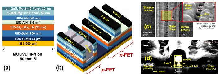
When compared with a planar channel, the fin channel has more surface area exposed to RIE plasma. Therefore, several steps were conducted to heal etch damage, namely, the following: 1) hot (75 ◦C) tetramethylammonium hydroxide (TMAH) treatment for 5 min, which was reduced from 15 min in to prevent complete etching of the highly scaled fins and 2) N2 treatment in a furnace at 500 ◦C for 30 min. This treatment resulted in a 15% improvement in channel resistance (hence, current level). The gate-stack was formed by the atomic layer deposition (ALD) of SiO2 (15 nm) using tris(dimethylamino)silane (TDMAS) and O2 plasma at 250 ◦C, and RF magnetron sputtering of Ti/Au (30/50 nm). The gate dielectric quality and p-GaN/dielectric interface make a significant contribution to the device switching characteristics, therefore making this an area of active research,. An optimized SA p-FinFET is presented in Fig. 1(c).

Fig. 1. Highly scaled GaN CT. (a) Epitaxial structure. (b) Device structures of p-FET (SA FinFET) and n-FET (SA-gate p-GaN-gate HEMT) based on the same GaN-on-Si platform, as illustrated in (a). (c) and (d) SEM images of representative p-FET and n-FET, respectively
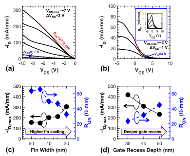
The performance of the p-FET with the best overall characteristics (LSD = 175 nm, LG SA, a fin width of 20 nm) is presented in Fig. 2. An ID,max of −300 mA/mm, an RON of 27 ·mm, and current saturation at high gate overdrive were achieved, as shown in Fig. 2(a). The transfer characteristics [Fig. 2(b)] reveal a Vth of 3 V and a peak transconductance, gm, of 13 mS/mm. The current ON–OFF ratio is 200, limited by the leakage current through the gate dielectric.

Fig. 2. Performance of p-FET and the scaling trends. (a) Output characteristics of p-FET with LSD = 175 nm (LG SA) and fin width = 20 nm. (b) Transfer characteristics of the abovementioned p-FET. The gm profile is presented in the inset. Study of the impact of (c) fin width and (d) gate recess depth on the performance (−ID,max and RON) of GaN p-FinFETs. −ID,max and RON were measured at VGS = −7 V.
The impact of two key device design parameters (fin width and gate recess depth) on DC output characteristics (ID,max and RON) was systematically studied for GaN p-FinFETs. As the fin width is reduced below 50 nm, the current density and RON improve [Fig. 2(c)]. However, this trend was not observed above 50 nm, possibly due to the significant reduction in the field-induced acceptor ionization effect. In addition, a deeper gate recess was found to reduce current density [Fig. 2(d)], primarily due to reduction of carrier density in the p-channel, but is expected to significantly improve ON–OFF ratio and subthreshold swing, as is the case for p-FETs based on similar epitaxial structures. Unfortunately, the gate oxide quality in this batch of fabricated transistors was found to be the limiting factor for the current ON–OFF ratio (<104 ). It follows that, the OFF-state characteristics were limited by gate control and drain-induced barrier lowering (DIBL), before a destructive breakdown at ≈20 V.
GAN N-FET: DESIGN AND CHARACTERIZATION
The SA gate process begins with the blank sputtering deposition of W (100 nm). Then, Ni/Au/Ni (30/120/80 nm) was patterned by electron beam lithography and liftoff. W was etched using the top Ni as a hard mask. Selective etching of p-GaN over AlGaN was achieved using SF6/BCl3 plasma, which has been reported to give high etch selectivity . W was chosen because of its high thermal stability (necessary for a gate-first process) and Schottky behavior with p-GaN gates . Finally, ohmic contacts were formed by Ti/Al/Ni/Au alloyed at 800 ◦C in N2 ambient. The typical contact resistance is ≈0.75 ·mm. A fabricated scaled SA p-GaN-gated n-FET is presented in Fig. 1(d). A proof-ofconcept layout was adopted, where the fabricated n-FETs are symmetric (gate is located in the center of the ohmic contacts, or LGS = LG D), and that electric field management structures (e.g., edge termination) were not included.
CONCLUSION
Advanced scaling based on SA features, as proposed in this work, offers a viable technology path for future high-performance GaN CT based on a MOCVD GaN-on-Si platform. The scaled p-FETs and n-FETs achieve competitive performance in their respective categories and, when taken together, deliver a leading GaN CT solution. Further design innovation and engineering of the proposed technology would greatly benefit the eventual wafer-level heterogeneous integration of GaN CT (based on a Si substrate) with Si CMOS to achieve multifunctional chips.
搜索“华林科纳行业观察”小程序查看完整内容,或者加微信13358064333/18106288187。