The application of thin underdense hydrogenated amorphous silicon (a-Si:H) films for passivation of crystalline Si (c-Si) by avoiding epitaxy in silicon heterojunction (SHJ) solar cell technology has recently been proposed and successfully applied. Herein, the microstructure of such underdense a-Si:H films, as used in our silicon heterojunction solar cell baseline, is investigated mainly by Raman spectroscopy, effusion, and secondary ion mass spectrometry. In H effusion experiments, a low-temperature (near 400 °C) effusion peak which has been attributed to the diffusion of molecular H2 through a void network is seen. The dependence of the H effusion peaks on film thickness is similar as observed previously for void rich, low substrate-temperature a-Si:H material. Solar cells using underdense a-Si:H as i1-layer with a maximum efficiency of 24.1% are produced. The passivation quality of the solar cells saturates with increasing i1-layer thickness. The fact that with such underdense material combined with a following high-quality i2-layer, instead of only high-quality a-Si:H with a low defect density direct on the c-Si substrate, good passivation of c-Si solar cells is achieved, which demonstrates that in the passivation process, molecular hydrogen plays an important role.
Introduction
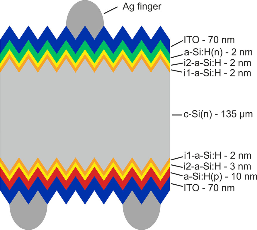
The use of porous a-Si:H films with high hydrogen content to prevent epitaxy has been proposed several times. Recently, such material was termed “underdense” by Liu et al.in connection with optical density measurements using the method of Remeš et al. “Underdense” means that the material has many large voids and low mass density in contrast to standard a-Si:H with a mass density of ≈ 2.29 g cm-3 . The mass densities of the a-Si:H films in this work are 2.1–2.2 g cm-3 and can therefore all be termed “underdense.” However, a reduction in density of (plasma grown) a-Si:H films for reduced substrate temperatures and/or enhanced hydrogen content is long known. It was found that in such material hydrogen diffusion is not by motion of H atoms but of H2 molecules. To clarify the microstructure of “underdense” a-Si:H, as used in SHJ solar cells,we applied Raman spectroscopy, hydrogen effusion, and other methods. We investigate layers of underdense a-Si:H with thicknesses from 2.3 to 150 nm grown at different plasma powers and on various substrates. We use effusion measurements in particular to compare the properties of the present a-Si:H with previously investigated a-Si:H material. Additionally, we used underdense a-Si:H for the i1-layer on the p-side of SHJ solar cells as shown in Figure 1 with a maximum efficiency of 24.1% on an area of (15.7x 15.7) cm2 . The i1-layer on the n-side was kept constant to ensure a clear comparison of the different i1-layers on the p-side.

Figure 1. Schematic of a SHJ solar cell and its layer stack.
Results
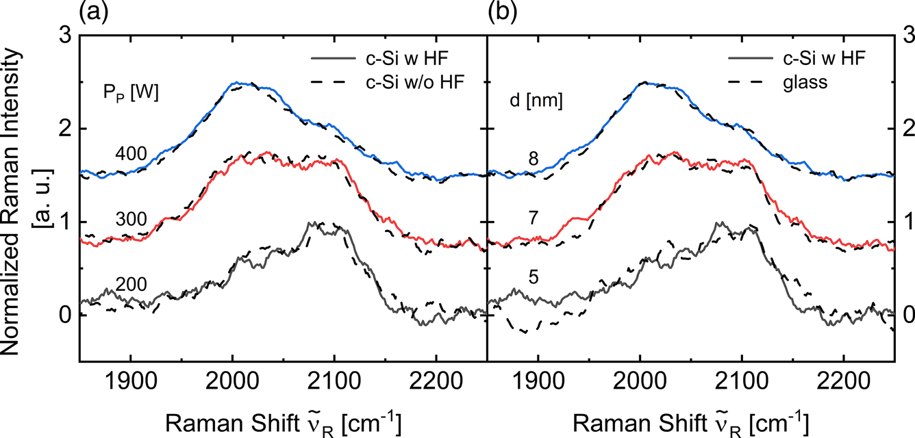
The growth of amorphous silicon layers can depend on the underlying substrate due to differences in nucleation.To investigate the growth process of underdense a-Si:H, we deposited films (d = 5–8 nm) using different plasma powers on HF-etched c-Si (with HF), c-Si with native oxide (w/o HF), and glass. Figure 2 shows the corresponding Raman spectra for wavelengths from 1900 to 2200 cm-1 . Three different plasma powers (200, 300, and 400 W) were applied, which were expected to result in different microstructures. Indeed, for the 200 W layer, the 2100 cm-1 peak is dominant, the 300 W layer shows a balanced ratio for the 2000 and 2100 cm-1 peak intensity, and for the 400 W layer the 2000 cm-1 peak is dominant. However, on all substrate materials, the spectra are similar, indicating a growth independent of the substrate material.

Figure 2. Raman intensity spectra normalized by its maximum of an intrinsic a-Si:H layer on a HF-etched c-Si substrate compared with a) a-Si:H layers from the same deposition on c-Si substrates with a native silicon oxide and b) a-Si:H layers from the same deposition grown on glass. The plasma power was varied from 200 W to 400 W in 100 W steps (indicated on the left in (a) resulting in thicknesses of 5 to 8 nm (indicated on the left in (b)).

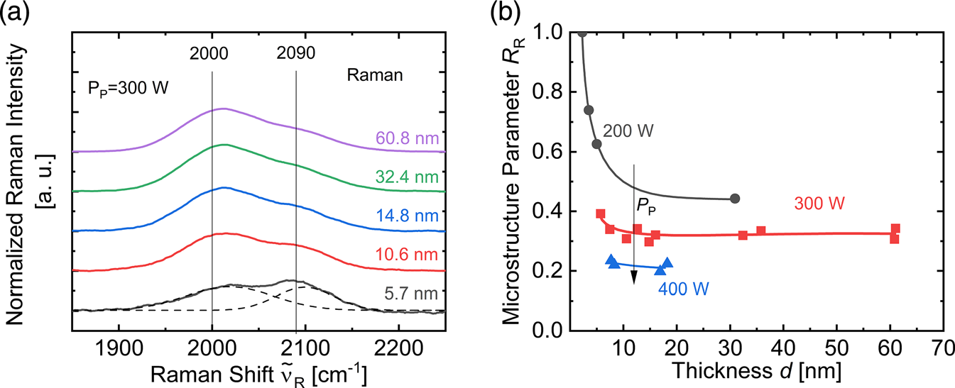
Figure 3. a) Raman spectra of intrinsic a-Si:H layers of various thickness deposited at PP = 300 W versus the Raman shift ˜νR. The sample thicknesses are indicated on the right side of the graph. The dashed lines show the double Gaussian function fits for the film of 5.7 nm thickness. b) Layer thickness dependency of R determined from Raman spectroscopy spectra of intrinsic a-Si:H layers with thicknesses of 2.3–60.8 nm and plasma powers of 200, 300, and 400 W. The lines are guides to the eye.
The microstructure parameter measured by Raman spectroscopy decreases with increasing plasma power, as shown in Figure 3, likely due to a different ion bombardment during film growth. With increasing film thickness d, R decreases for films d < 10 nm and is constant for films d > 10 nm. Using the method of Remeš et al.with H concentration from infrared absorption, the density of our films with d > 10 nm is 2.1 g cm-3 for the 200 W film, 2.16 g cm-3 for the 300 W film, and 2.2 g cm-3 for the 400 W film. The density of films with d < 10 nm (not given, since the H content determined by FTIR is very uncertain for these films) can be significant lower, which agrees with the increase of R at lower thickness d indicating a void-rich film. This increase of R can be assigned to a different microstructure of the nucleation layer of the a-Si:H film,showing that the nucleation layer of our underdense material is smaller than 10 nm.
Discussion
Underdense a-Si:H is used as i1-layer in the SHJ solar cell fabrication. This layer is intended to improve the passivation of the c-Si surface by avoiding an epitaxial growth using a fast (>1 nm s-1 ) and disordered growth instead. The similar Raman spectra of layers grown on different substrate during one deposition process with thicknesses of 5 to 8 nm shown in Figure 2 agree with a lack of epitaxy. For layers including epitaxial growth on the HF-etched c-Si surface, a strongly reduced H content and a microstructure parameter close to 1 would be expected. The microstructure of the (nonepitaxial) layer on the glass substrate would be significantly different. The similar Raman spectra for layers on different substrates therefore indicate a similar growth mechanism for all investigated substrate materials resulting in a void rich material in particular at low plasma power, presumably due to the rather low self-bias. R measured by Raman spectroscopy is thickness independent for layers above 10 nm, while R rises for layer thicknesses <10 nm. This latter increase is likely related to an a-Si:H nucleation layer. The presence of a nucleation layer of about 10 nm or less has also been modeled by, Canillas et al., Fujiwara et al., and Li et al.. Furthermore, the solar cell results show that the island-like growth during the nucleation already results in a wide area covering film for thicknesses > 2 nm since the passivation quality for i1-layers with di1 > 2 nm is constant. The high microstructure parameter (especially for films <5 nm) shown in Figure 3 and the effusion peak near 385 °C as well as the plateau-like H diffusion SIMS profiles for annealing at 400 °C in Figure 4 show that our “underdense” films are highly porous and the H diffusion is dominated by molecular H2 instead of atomic H. In agreement with this, recently An et al. also stated that the passivation quality highly depends on the low-temperature H effusion characteristics. This indicates that for the good passivation as achieved with underdense a-Si:H, the c-Si is passivated by dissociative absorption of H2 and not by diffusion of atomic hydrogen to the silicon dangling or reconstructed bonds. This agrees with the fact that the passivation is independent of the i1-layer thickness for di1 > 2 nm as shown in Figure 5, since a thicker i1-layer would hinder the atomic H diffusion from the i2-layer. The role of the second, more dense a-Si:H i2-layer, which is needed to achieve high passivation in combination with the i1-layer, may be to keep the H2 next to the c-Si surface.
Conclusion
The “underdense” a-Si:H resembles both in Raman and H effusion the “low-temperature” a-Si:H, whose properties have been discussed extensively in the past. The high H concentration and porosity of this material apparently prevent epitaxy. Varying the thickness of the underdense i1-layer on the rear side of our solar cells, we achieved a maximum efficiency of 24.1%. Our material investigation shows that hydrogen diffusion in underdense a-Si: H is mainly by molecular H2. Therefore, the successful passivation mechanism of underdense a-Si:H in direct contact with c-Si is probably due to mobile H2 molecules rather than diffusion of atomic H. We propose that the underdense structure facilitates H2 diffusion to the interface between c-Si and a-Si:H. The dissociative adsorption of H2 molecules leads to the silicon passivation at the interface.
搜索“华林科纳行业观察”小程序查看完整内容,或者加微信13358064333/18106288187。