用湿法腐蚀法从块状锗衬底上制备亚10 um厚的锗薄膜
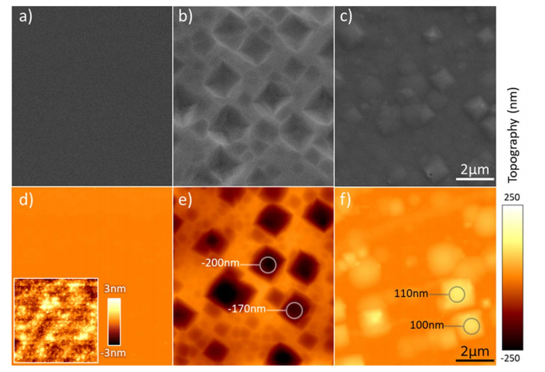
Low-detect density Ge thin films are crucial for studying the impact of deect density on the pertormance limits ofGe-based optical devices (optical detectors, LEDs, and lasers ). Ge thinning is also important for Ge-based multijunction solar cellsIn this work, Ge wet etching using three acidic H,O, solutions (HF, HCl, and H,SO ) was studied in terms of etching rate, surfacemorphology, and surface roughness. HCI-H,O,-H,0 (1:1:5) was demonstrated to wet-etch 535 ym-thick bulk-Ge substrates to4.1 um with a corresponding RMS surface roughness of 10 nm, which was the thinnest Ge flm from bulk-Ge via a wet etchingmethod to the best of our knowledge.

用过氧化氢电解蚀刻锗基板
Anodic electrolytic etching of germanium has been performed in hydrogen peroxide etchants with controlled external conditions.In-situ current and ex-situ etch-depths were measured and tracked with respect to etchant composition and stir rates. Gas bubblesformed during the etching process were found to cause non-uniformity in etch-current and surface quality. The effects were
minimized in specific composition spaces. Quantitative analysis revealed a linear correlation of the number of electrons transferred during germanium oxidation with the number of surface atoms removed. Experimental results of 2.77 electrons/atom deviate significantly from 4 electrons/atom previously reported for silicon.

不同厚度硅衬底的 Cu 电镀 GaN_AlGaN 高电子迁移率晶体管的热性能
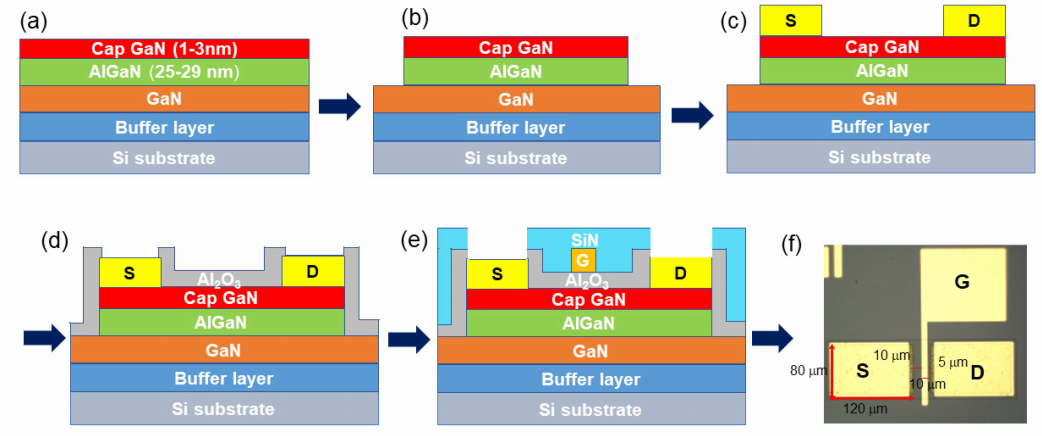
Thermal dissipation is an important issue for power devices. In this work, the impact of thermal effects on the performance of Cu electroplated GaN-based high-electron-mobility transistors (HEMTs) are considered. Electrical, thermometry and micro-Raman characterization techniques were used to correlate the effects of improved heat dissipation on device performance for GaN HEMTs with different thicknesses of Si substrate (50, 100, 150 µm), with and without an additional electroplated Cu layer. GaN HEMTs on electroplated Cu on Si (≤50 µm) demonstrate an enhanced on/off current ratio compared to bare Si substrate by a factor of ∼400 (from 9.61 × 10⁵ to 4.03 × 10⁸). Of particular importance, surface temperature measurements reveal a much lower channel temperature for thinner HEMT devices with electroplated Cu samples compared to those without.

关键词:锗薄膜,块状锗,湿法刻蚀锗,刻蚀锗,电解刻蚀,过氧化氢,高电子迁移率晶体管,GaN_AlGaN,Cu 电镀、氮化镓、HEMT、电镀铜、拉曼测温法,硅衬底