Abstract— This letter describes a direct Cu bonding technology to there-dimensionally integrate heterogeneous dielets based on a chip-on-wafer configuration. 100-µmcubed blue µLEDs temporarily adhered on a photosensitive resin are interconnected by semi-additive plating (SAP) without thermal compression bonding. By using SAP bonding, a lot of dielets can be stacked on thin 3D-IC chiplets. The following three key technologies are applied to solve the yield issues of SAP bonding. After pickand-place assembly, additional coplanarity enhancement eliminates Cu bridges grown to a small gap between the µLEDs and photosensitive resin. The µLEDs arrays with sidewalls insulated by room-temperature ozone-ethyleneradical (OER)-SiO2-CVD are successfully bonded on sapphire wafers and a thin 3D-IC with through-Si via (TSV). Further design optimization is required, but partial seed pre-etching works well to increase the yield. Fully integrated module implementation with the 3D-ICs will be the next stage, however, we discuss a superior prospect for yield enhancement toward nearly 100%.
I. INTRODUCTION
HETEROGENEOUS integration studies have been started by monolithic stacking of III-V device on Si or GaAs wafers for optoelectronic applications . Until the late 1990s, conventional heterogeneous integration had been limited to the fabrication of heterojunctions, e.g., GaAs/GaAlAs. Over the past two decades, flip-chip bonding technology with small chips has been widely used in industry, and heterogeneous integration research has been extended to other fields such as microelectromechanical systems (MEMS) and sensors . Meanwhile, heterogeneous integration works have been moving beyond 2D structures to 3D . More recently, 3D-DRAM has been split into several high-bandwidth memory (HBM) and integrated with CPU. Such a heterogeneous integration architecture is increasingly used to three-dimensionally stack logic chips manufactured at different technology nodes.
Nowadays, these chips called chiplets are expected to be a promising driver to advance not only size scaling according to Moore’s law but also performance scaling. Chiplets are Si intellectual property subsystems and do not simply indicate small chips divided from a large system on a chip. They are intended to be interconnected with advanced microelectronic packaging technologies such as redistributed layer (RDL), solder microbumps, and TSV to build complete functionality.
Based on fan-out wafer-level packaging (FOWLP), we have proposed “Smart Skin Display” as a flexible µ LED display with wearable vein viewers and sensors consisting of nearIR/red mini-LEDs and a 3D-IC chiplet array on which blue µ LEDs are stacked and interconnected with TSV . We call the heterogeneous chiplets “dielets” that involve tiny dies, including optics, MEMS, and passives in addition to standard chiplets. This FHE embedding the heterogeneous dielets can monitor vascular information as a predictor of blood clots etc., from the light emitted by the mini-LEDs. The reflected light from hemoglobin is detected with photodiodes designed in the 3D-IC dielets that process and transfer the resulting signals to LED drivers in the 3D-IC to drive the stacked µ LEDs.
II. FABRICATION
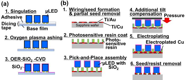
Fig. 1 shows the process flow of SAP bonding with incoming µLEDs. The 100-µm-square µLEDs have a 6-µm-thick active GaN layer and approximately 100-µm-thick sapphire substrate. The electrode size of the µLEDs is 25 × 75 µm2 for both the anode and cathode, and the inter-electrode distance is 25 µm.

Fig. 1. A process flow of micro-LED sidewall insulation in tape-level processing (a) and SAP bonding (b). cussed for this FOWLP-based flexible and 3D heterogeneous integration.
The µLEDs were attached to a dicing tape in a face-down fashion. First, the sidewalls of the µLEDs singulated by laser cutting were insulated with a 100-nm-thick SiO2 deposited by room-temperature OER-SiO2-CVD (Meiden Nanoprocess Innovation) with tetraethoxysilane at the dicing-tape level. Since such blue tapes were composed of a glue layer and base film, the GaN layer was partially covered with the glue with a thickness of 10 µm. Before OER-SiO2-CVD, an ashing process was added to fully expose the GaN sidewall. The glue layer surrounding the µLEDs was removed by O2 plasma (300 W/10 min).
III. RESULTS AND DISCUSSIONS
Fig. 2 shows SEM images of a µLED array after SAP bonding. The µLEDs are interconnected to Ti/Au wirings through electroplated Cu pillars. The alignment accuracies in XY directions are found to be ±10 µm, and the maximum angular alignment error is 7◦ . The XY positional accuracies ±10 µm are acceptable even with the worst angular error, considering that, for example, highly reliable results have been obtained for fine-pitch microbump interconnections with an inter-bump space of 5 µm. The alignment errors would slightly increase DC resistance to drive the µLEDs through the Cu pillars. The increased DC resistance is added to onresistance, but there is no significant positive shift in threshold voltages (VT H ). This alignment errors seem not to be related to SAP bonding failures described below. Thus, the assembly (alignment) yield can be said to be 100%.

Fig. 2. SEM of a µLED array after SAP bonding (a), a magnified bonded µLED (b), and the cross-section of a µLED with sidewall insulation (c).
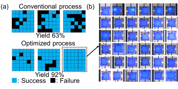
However, the yield of interconnection is 63% in the first bonding trial with a conventional process listed at the top of Fig. 3(a). Three blocks of each 6 × 6 µLED array are extracted, and whether the µLEDs emit blue light is mapped. The bottom of Fig. 3(a) shows the interconnect yield of the µLEDs bonded under current conditions used in this study where three key technologies, 1) µLED sidewall insulation, 2) additional tilt compensation, and 3) partial seed pre-etching, are used to enhance the yield. The interconnect yield eventually increases up to 92% with the new process.

Fig. 3(b) shows the optical microscope images of emitting blue light from the µLEDs taken during I-V measurement. The 6 × 6 µLED array block is picked up from the bottom right in Fig. 3(a). All the µLEDs emit blue light, although there are variations in electroluminescence intensity.
The sidewall insulation of the µLEDs prevents the active GaN layer from electrical short with excess growth of electroplated Cu. When µLEDs without sidewall insulation are bonded, the electroplated Cu, once it reaches the Au electrodes of the µLEDs, is further grown from the GaN sidewall. However, low-temperature processes are required for sidewall protection after the singulation process. Typically, the glue layers of dicing tapes are not thermally stable. Therefore, room-temperature OER-SiO2-CVD is employed to enhance the interconnect yield with the good quality of SiO2 . Additional compressive force after chip placement eliminates a small gap between the photosensitive resin and tilted µLEDs, preventing the generation of Cu bridges connecting the p- and n-type Au electrodes. The coplanarity of the tilted µLEDs is also improved. Furthermore, it is difficult to promptly etch the seed layer at the hidden parts underneath the µLEDs. The partial pre-etching of the Cu seed before µLED placement reduces the defects derived from excess Cu pillar undercut/thinning in the seed removal step after SAP bonding.
The I-V characteristics of the µLEDs after SAP bonding are shown in Fig. 4, where the I-V behaviors are mainly classified into three categories. The representative I-V curves of the three µLEDs are exhibited with inset microscope images. Figs. 4(a) and (b) show the I-V characteristics of the 1st and 2nd µLEDs with excellent and relatively lower electroluminescence intensity. The 2nd µLED gives one orders of magnitude lower intensity than the 1st µLED when the voltage is increased up to 3 V. However, they are at a similar level as the pristine µLED dies before SAP bonding. Therefore, the difference in the intensity of the µLEDs between Figs. 4(a) and (b) is due to initial characteristics variation resulting from LED wafer fabrication processes, not due to the impact of SAP bonding. Here, we skipped the wafer test step for known good die selection to make their luminescence intensity uniform. The current flowing to the negative voltage region is the same level as the 1st µLED, which means there is no leakage. On the other hand, Fig. 4(c) shows the I-V curve of the 3r d µLED having considerably low emission intensity. The current is not sufficiently running.

Fig. 4. I-V characteristics of intense-emission (a), weaker-emission (b), and weakest-emission (c) µLEDs before and after SAP bonding.
As seen in Fig. 5(a), the image taken by a fluorescence microscope exhibits dark emission from the 3r d µLED. The emission intensity of the 1st and 3rd µLEDs are compared using X-ray transmission images, as shown in Fig. 5(b). Small voids are observed in an intense-emission µLEDs, but there is no resistance increase to positively shift the VT H . In contrast, no voids are observed when the weakest-emission µLEDs are taken. The reason why the emission of the 3r d µLED is extremely low is thought to be small leakage at the pre-etch parts, as mentioned below.

Fig. 5. Fluorescence microscope (a) and X-ray transmission (b) images of intense-emission (left) and weakest-emission (right) µLEDs.
As seen in Fig. 5(a), the image taken by a fluorescence microscope exhibits dark emission from the 3r d µLED. The emission intensity of the 1st and 3rd µLEDs are compared using X-ray transmission images, as shown in Fig. 5(b). Small voids are observed in an intense-emission µLEDs, but there is no resistance increase to positively shift the VT H . In contrast, no voids are observed when the weakest-emission µLEDs are taken. The reason why the emission of the 3r d µLED is extremely low is thought to be small leakage at the pre-etch parts, as mentioned below.
IV. CONCLUSION
We developed a room-temperature direct Cu interconnect technology “SAP bonding” to heterogeneously integrate tiny dies with 3D-ICs. µLED arrays were emitted on sapphire wafers using a dielet-on-wafer 3D integration, and 6 × 6 µLEDs were stacked on a thin 3D-IC without mechanical failure. OER-SiO2-CVD and partial seed preetching were very effective to increase the interconnect yield, but the design should be further optimized in the next 3D heterogeneous integration with thinned 3D-IC arrays with TSV.