ABSTRACT
Reducing both the cost and weight of Germanium (Ge)-based devices is a key concern in extending these technologies to mainstream applications. In this framework, the porous Ge liftoff, based on a mesoporous Ge layer (PGe), shaped by bipolar electrochemical etching (BEE), constitutes an appealing strategy allowing the separation of lightweight, flexible, and low-cost devices and substrate reuse. However, after the device detachment, the broken pillar residues on the host substrate’s surface prevent its reuse. Here, we report on the development and application of a reconditioning process based on an aqueous HF:H2O2:H2O (10:80:10, v-v-v) mixture without the need for Chemical Mechanical Polishing (CMP). We found that a mixed kinetic- and diffusion-controlled wet etching leads to surface polishing. Flat reconditioned substrates with low surface roughness (<2.5 nm RMS) are successfully obtained from detached surfaces with various pillar sizes up to 500 nm in diameter. The substrate reusability is demonstrated by achieving a new porous layer on a reconditioned substrate with an RMS roughness of 2.2 nm, ready for a second round of the membrane’s epitaxial growth. These results demonstrate a CMP free, reliable Ge substrate reconditioning process, paving the way towards substrate multi-reuse and consequent devices' weight and cost reduction.
1. INTRODUCTION
Germanium (Ge) is a material of choice for the design of various devices such as batteries and biosensors. However, it is mostly used as a platform for III-V materials integration for high-power-density optoelectronic and photovoltaic (PV) devices. Substrates of this rare and critical material represent approximately 30-40% of the overall device cost, preventing its large-scale adoption for mainstream terrestrial PV applications. Although standard 100 mm Ge wafers have a thickness of around 175 µm, the absorber thickness is much thinner (~2-5 µm), resulting in a substantial part of the Ge substrate being used only as a mechanical support for manufacturing. This substrate thickness results in a significant cell weight, which is another challenging factor, especially for space PV applications, and may require being thinned down . Furthermore, wasting Ge material is undesirable from an environmental perspective. These technological, economic, and sustainable considerations are calling for the development of a process flow that reduces the consumption of Ge, while targeting lightweight and low-cost devices.
2. METHODS
2.1. Ge samples and solutions:
P-type gallium-doped, 100 mm Ge wafers with resistivity 7-30 mΩ·cm and (100) crystal orientation with 6° miscut towards (111), as well as hydrofluoric acid (HF, 49 wt.%), hydrogen peroxide (H2O2, 30 wt.%), hydrochloric acid (HCl, 37 wt.%), ammonia solution (NH4OH, 20-30 wt.%), ultrapure water (H2O), and ethanol (EtOH, 99 wt.%) are used in this study.
2.2. Porous lift-off process:
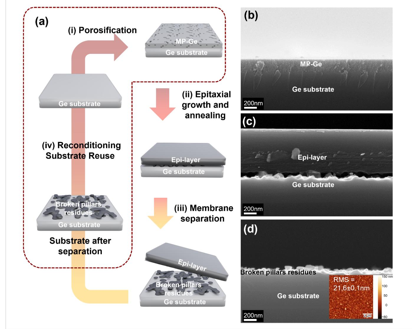
The porous lift-off process flow used in this study is based on the PEELER process reported in our previous work and is described in Fig. 1 (a). (i) A PGe layer is shaped by electrochemical etching on top of a Ge wafer (Fig. 1 (b)). (ii) After porosification, the Ge membrane (NM) is grown on top of the porous structure with a two-step growth. The thermal budget during epitaxy leads to the reorganization of the PGe layer into pillars separated by voids. A typical cross-sectional scanning electron microscope (SEM) image of the obtained structure after epitaxy is shown in Fig. 1 (c). The epitaxial Ge layer exhibits a single crystal quality (Fig. S1) with low surface roughness (< 1 nm RMS, Fig. S1). (iii) Finally, the crystalline Ge NM is separated from the substrate by means of the voided-separation layer, using normal mechanical pulling. During this separation method, the stress accumulation due to the mechanical pulling will initiate cracks in the pillars, allowing the NM release. Consequently, as shown in Fig. 1 (d), the NM detachment leaves broken pillar residues on the detached surface of the mother substrate, leading to a high RMS roughness above 20 nm, measured by atomic force microscopy (AFM) presented in the inset of Fig. 1 (d).

Fig. 1: (a) Process-flow of the porous lift-off approach. (b) SEM cross-sectional image of a porous layer. (c) SEM cross-sectional image after the epitaxial growth. (d) SEM cross-sectional image of the Ge substrate after NM separation, with a typical AFM scan as inset.
2.6.Ge surface wet etching:
Wet etching experiments are conducted at room temperature with a rotation rate of 600 RPM. The etch rates are determined by a lithographic process of patterned stripes and profilometer measurements before and after the wet etching on bulk Ge wafers. Since the targeted substrates to be reconditioned have nanostructured surfaces with only tens of nm average height, and considering the µm-scale etched depth, the obtained etch rate on PGe samples is considered the same as those determined for the bulk Ge wafer. All ratios shown in this study are volume ratios (v-v-v). Based on the determined etch rate, we selected the etching time to achieve a 5 µm thickness removal of Ge. The etching depth has been verified using profilometer measurements.
3. RESULTS AND DISCUSSIONS
3.1. Wet-etch-reconditioning process development:
In contrast to bulk Ge, the nanostructured Ge is characterized by a large surface area, which induces a different reactivity compared to a bulk substrate. To shed light on the polishing behavior of the different mixtures on nanostructured non-epi-ready Ge wafers, we first consider fresh PGe samples as test vehicles to determine a suitable composition mixture to recondition the detached wafers. To determine the most suitable composition for reconditioning purposes, three typical mixtures have been tested on PGe: (1) dilute Ammonia Peroxide Mixture (APM, NH4OH:H2O2:H2O, 1:1:5, v-v-v), (2) dilute Hydrochloric acid Peroxide Mixture (HPM, HCl:H2O2:H2O, 1:1:7, v-v-v), and (3) HF-based solution (HF:H2O2:H2O, 1:3:6, v-v-v). After APM and HPM etching, the surface exhibits a rough topography with the presence of either GeOx-based crystals or residues, making these solutions unsuitable for reconditioning purposes (Fig. S2). Conversely, after HF-based solution etching, a defect-free surface is obtained after PGe etching. The rest of this study will focus on this type of mixture.
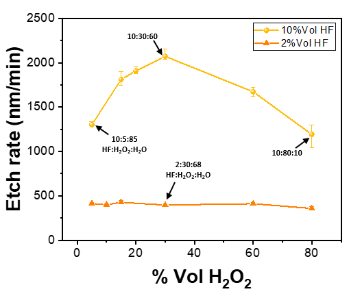
The etching behavior of the HF-based solutions on nanostructured Ge has been further investigated to determine a solution suitable for our reconditioning process. Fig. 2 represents the etch rates obtained on bulk material for an HF volume percentage equal to 2% and 10% as a function of the volume percentage of H2O2, completed with water to keep both the HF concentration and the mixture’s volume constant. From these measures, it is evident that when using solutions with 2%Vol of HF, the etch rates are relatively low (<500 nm/min) and not affected by the volume percentage of H2O2. Interestingly, for higher 10%Vol of HF, the etch rate is found to increase first with increasing the %Vol of H2O2, reaching a maximum of 30%Vol before decreasing monotonously. The increasing etch rate domain seems to be governed by an excess HF regime and the etching is then limited by the oxidation of the surface. Conversely, for a higher %Vol of H2O2, a uniformly oxidized surface can be formed and subsequently dissolved [39]. The etching of the oxidized Ge-based compounds becomes the rate-limiting step of the etching process. The decrease in the etching rate is likely due to the higher proportion of H2O2 in the stagnant film present on the surface of the substrate, which will induce a higher mass-transfer control of the HF etching at the surface of the Ge [40]. In addition, increasing the H2O2 concentration could also favor the formation of Ge-OH bonds instead of Ge-F formed when Ge surface atoms are in contact with HF. Due to the higher electronegativity difference between Ge and F than between Ge and O (2.0 Vs 1.4), the Ge-F bond is supposed to be more ionic than the Ge-O. This polarizing nature of Ge-F weakens the back bond and induces a Ge atom release. The increase in Ge-OH quantity by increasing 11 the H2O2 proportion has a surface stabilization effect and reduces the etch rate at fixed %Vol of HF.

Fig. 2: Etch rate as a function of %Vol of H2O2 for 2%Vol HF (orange triangles) and 10%Vol HF (yellow dots) on Ge bulk material (room temperature, 600 RPM). For more details, four mixture compositions are indicated (HF:H2O2:H2O, v-v-v).
The nanostructured Ge etching can be separated into two etching steps: the nanostructure etching followed by the bulk material flattening. During the nanostructure etching, a substantial amount of Ge (hydro)suboxides can accumulate on the nanostructure surface. These suboxides can hamper the etching due to their limited solubility. These deposits cause high surface roughness, as observed with a low %Vol of HF, and make this etching domain unsuitable for the substrate reconditioning process (Fig. S3). To avoid this anisotropic behavior, while maintaining the etching rates in the order of a few µm/min, the volume percentage of HF is then fixed at 10%Vol to increase the desorption/dissolution rate of these oxidized compounds.

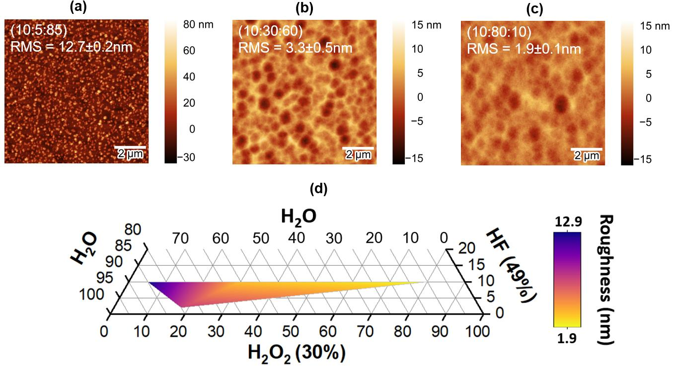
Fig. 3: AFM scans after PGe etching with different HF:H2O2:H2O volumetric ratios: (a) 10:5:85 (b) 10:30:60 (c) 10:80:10 after 5 µm of etching. (d) Triphasic diagram of the roughness vs. reagent %Vol.
Fig. 3 (a-c) shows AFM scans and RMS roughness of PGe samples after wet etching with different HF:H2O2:H2O volumetric ratios. These etched surfaces are obtained after only 5 µm of etching, i.e., 3 min 51 s, 2 min 59 s, and 4 min 12 s of etching, respectively (Fig. 2). With a lack of oxidizing agents (H2O2 < 30 %Vol, Fig. 3 (a)), the oxidation is non-uniform across the surface of the nanostructure, and a strong anisotropic etching is observed. As a result, a high roughness of 12.7 ± 0.2 nm (Fig. 3 (a) and Fig. S3) indicates that this etching domain is unsuitable for the reconditioning process. Conversely, when the oxide layer can form homogeneously (H2O2 > 30 %Vol, Fig. 3 (b-c)) on the entire surface area of the nanostructured PGe, all the surface structures are efficiently removed, and a flat surface with a roughness of 3.3 ± 0.5 nm is obtained using a 10:30:60 (HF:H2O2:H2O) solution (Fig. 3 (b)).
4.CONCLUSIONS
In this work, we investigate three different mixtures based on dilute ammonia peroxide mixtures, dilute hydrochloric acid peroxide mixtures, and HF-based solutions as a potential alternative to the costly CMP process for Ge substrate reconditioning after the porous lift-off process. HF:H2O2:H2O mixtures exhibit a polishing behavior of nanostructured Ge, and an experimental demonstration of substrate reuse has been established. With the investigation of the etching mechanisms involved in the polishing of nanostructured Ge surfaces, a solution with a volume ratio of (10:80:10) was determined to be suitable for substrate reconditioning. The robustness of our approach was tested on surfaces with pillar diameters ranging from 37 nm up to 500 nm obtained after post-growth thermal annealing at various temperatures. We succeeded in smoothing the detached Ge substrate by chemical etching and obtaining a low surface roughness (< 2.5 nm RMS) after only 5 µm of etching, regardless of the initial surface morphology, proving its compatibility with porous and other lift-off techniques. Using this reconditioning process, we obtained a porous layer ready for epitaxy with characteristics identical to those obtained on epi-ready substrates (thickness, morphology, and porosity) and a low surface RMS roughness of 2.2 ± 0.2 nm.