Electronics are in a transitional phase where 2D electronics are losing their capability to keep up with Moore’s Law. 3D integration is the next step that allows the continuation to improve efficiency in electronics. Vital technology to stack the microchips on top of each other that have previously been placed side-by-side is through-wafer-interconnects. These vias allow chips to be electrically connected with short interconnect length and without the need for traditional wirebonding. This thesis aimed to explore the possibilities of wet etch process modification for copper filled TSVs to improve seed layer deposition and electroplating process steps. TSVs were fabricated by Bosch etch and post-process tests involved various mixtures of HF/HNO3 solutions. TSVs were characterized empty and filled with copper by optical and electron microscope to see post-process effect on via and modification effect on copper filling. Roughness improvement by wet etching proved to be challenging and better results are obtained by optimizing dry etch parameters for minimal roughness. Profile improvement proved to be successful and repeatable with more diluted HNA solutions.
1 Introduction
User’s continuous demands for miniaturized handheld devices are ever increasing the need for new methods in electronics manufacturing. These demands include reduced signal delay, broader bandwidth, better power management and more compact package areas. Three dimensional (3D) wafer-level integration, 3D integration or 3D integrated circuits (IC), is the next technology that allows Moore’s Law to continue meeting these demands. In 3D integration multiple devices on separate wafers are stacked together vertically. What used to be microchip board is now becoming a single microchip. The chips on these wafers are interconnected by these through-vias instead of wirebonds or tape automated bonds like the two dimensional (2D) chips. Richard Feynman and William Shockley first introduced these vias and the concept of 3D integration already in 1960s through their patent "Semiconductive Wafer and Method of Making the Same" which was granted 1962. This idea was further developed by IBM researchers Merlin Smith and Emanuel Stern that started talking about thru-connections in their patent that was granted in 1967. However, the first 3D integrated chip utilizing this technology was developed 17 years later in 1983 Japan by Hitachi which makes this technology 40 years old at the time of writing.
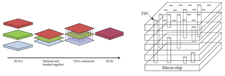
Despite existing for so long 3D integration is rising to prominence in 2020s. Developing technologies on design and fabrication processes has made 3D integration more available in compatibility and price while 2D ICs are losing their momentum. One could see that we are today in an intersection where old technology is still viable and cheaper, yet if the same technological progress is to be maintained new generation of integration needs to be implemented categorically in electronics. This demand creates and grows new markets that maintains strong incentive to develop through-silicon-via (TSV) technology. Figure 1 demonstrates the transition from 2D to 3D and how TSVs are connecting these layers.

Figure 1: One the left is shown how multiple chips are made one and on the right how these device layers are connected in various ways by TSVs.
There are vias with diameters 1 µm - 200 µm and depth from some tens of microns to holes that go all the way through the wafer. Since wafer thicknesses can be over 600 microns there are vias that are almost 1:100 in width and depth making them extremely narrow. This relation of width to depth is called aspect ratio (AR) and it is one of key features of TSVs. The shape and scale of the cavity affects on how the etch proceeds. Wide trenches and large cavities are exposed to larger quantities of gas and etches faster. Small round holes has constricted access, therefore they etch slower and less uniformly. When fabricating these vias on a wafer, one has to design how densely they are packed which is largely limited by the via dimensions. Wider and deeper vias needs more space and they might get enlargened in process steps after forming the original via. Different vias can be fabricated in a single batch that is pictured in figure 2a. 2b shows the usual patterning of arrays on a silicon wafer where space is left on all sides of the wafer for handling. 2c shows more modern blind via and true TSV.

Figure 2: a) 40 smaller 5 µm vias can incorporate the same space as 25 or 14 vias with 10 µm or 15 µm widths, respectively b) One square represents a batch from 2a c) Blind vias stop inside the wafer, through-wafer-via goes actually through the whole wafer.
Vias can be etched either by plasma etching, also known as dry etching, or wet etching that implies the use of liquid solution to remove silicon. Physical dry etching utilizes particle beams where the kinetic energy of ions in collision to substrate surface remove atoms from surface which is called sputtering. In chemical dry etching gaseous solutions are used in short pulses that either etch or deposit material while ions are accelerated from plasma towards the substrate by bias voltage. These ions sputter away materials they hit by line-of-sight. Therefore, they do not hit the sidewalls of a via leaving deposited passivating films to protect from etching gas resulting in removal of silicon only in horizontal direction.
Fabrication of blind vias that is used in this study present major challenges in process control. Dry etching is able to produce great variety of shapes and surfaces, yet each goal in structure demands very specific process parameters that can often exclude achieving multiple targets simultaneously. Liquid etching can complement these shortcomings as a post-process. However, liquid etching in itself is difficult to control and does not present a large margin of variety.
2 Through-silicon-vias (TSV)
Through-wafer-interconnects are an integral technology in 3D-packaging. While sometimes called generally through-chip-vias (TCVs), for silicon substrate they are called through-silicon-vias (TSVs) and for glass substrates they are known as throughglass-vias (TGVs). As the name implies it is a hole that goes through substrate connecting both surfaces. If the hole in silicon wafer is filled with conducting material and chips bonded on both sides of the TSV it becomes an interconnection connecting those two chips electronically together. Filling conducting material can be doped polysilicon in earlier process steps which allows high temperatures. Tungsten can be used for high aspect ratio via in CMOS since it possesses excellent step coverage with W F6 based chemical vapour deposition (CVD) chemistry and tungsten has good compatibility with CMOS transistors. Copper is used almost exclusively for everything else. However, Cu is an unwanted trace metal in active devices, so its inclusion in TSVs requires many precautions complicating processing significantly.
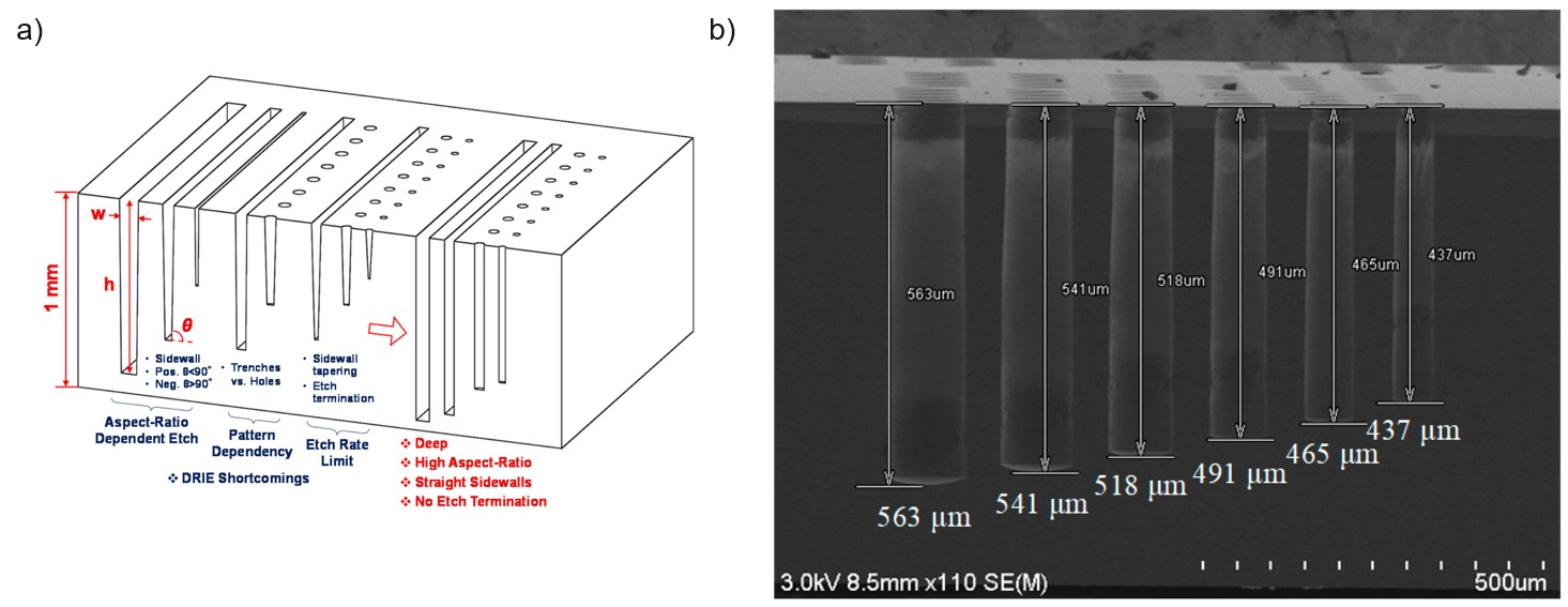
Most common fabrication method for TSV is deep reactive ion etching (DRIE), which is the extension of reactive ion etching (RIE), and it is our chosen method as well because optimal surface roughness is the key goal in our process. The foremost benefit of DRIE is the ability to produce high aspect ratio sidewall cavities that are very well suited for TSVs. There are a variety of TSV shapes (figure 3) that can be selected based on application where they are used. The process can also be optimized for smooth sidewalls that produces peak-to valley sidewall roughness in nanometers. DRIE will be discussed on Microfabrication section in more detail.

Figure 3: a) Shape, size and the pattern of the cavities determines which fabrication challenges needs to be overcome b) Wider hole induces higher etch rate that leads to deeper via.
In 3D chip the total data transfer rate, the bandwidth, is defined by the number of stacked TSVs. However, the coupling effect increases the more densely the TSVs are packed which starts to affect the bandwidth negatively [8]. As a general rule, square shape yields more bandwidth by better packaging but round shape induces significantly less stress that is often more crucial. Therefore, rectangular trench can conduct more efficiently but introduces reliability issues. Trenches and vias are compared in figure 3a. The picture shows if all these cavities are fabricated on the same wafer with same etch. Due to different phenomena that becomes from variety of cavity shapes, the depth and sidewall profiles differ significantly. Figure 3b shows that adjusting via height can be done with relative ease by changing cavity width. However, this forces the holes to a certain aspect ratios. Same etching round can not produce holes of arbitrary sizes and multiple dry etches on same areas is to be avoided.
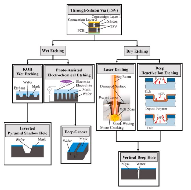
Different fabrication methods are depicted in figure 4. Anisotropic wet etching using a base such as potassium hydroxide (KOH) or tetramethylammoniumhydroxide (TMAH) produces inverted pyramid shaped hole. The sidewall angle is 54.7 ◦ , therefore aspect ratio and depth are severely limited. To fabricate 500 µm deep via with 10 µm hole on the backside, the hole on the front side of the wafer would be over 700 µm wide. Therefore, anisotropic wet etching method is used for very large and shallow vias.

Figure 4: Choosing any of the methods will have its advantages and disadvantages. DRIE etch is the most popular choice today.
3 Wet etching
To manufacture ever smaller electronic components we have long since hit the inevitable threshold where our traditional mechanical tools are simply too large. For us to continue to pursue downscaling of electronics, especially the ICs, new tools were constantly innovated or in this case ancient tools brought to modern times. Developed in antiquity for copper engravings, wet etching is still used today for microfabrication of modern electronics. In the early days of IC development it was the only etching used where nowadays gas phase plasma etching is often the preferred method. Wet etching is either fully isotropic or anisotropic between crystallographic planes and both have limitations in the range of different shapes as well as the scale they are able to produce. Nevertheless, when the process is controllable and repeatable wet etching does provide simple approach for fabricating structures on a whole batch of wafers which is much less time consuming than etching a single wafer at a time. Wet etching is simple and cheap method to operate versus dry etch. However, cheap applies to start up and running costs. When comparing DRIE to anisotropic KOH wet etching, it yields more than twice the chips per wafer making cost per chip less. Therefore, the batch fabrication by wet etching has somewhat higher throughput and cost per wafer is lower. Cost per chip is lower for DRIE which means that production costs’ ratio for profit per wafer is lower. The control is most often inferior in wet etching to dry etching as well so a greater tolerance for error is needed.
A definition for etching is the removal of solid material, often this is done by chemical reaction. If etching is performed by a liquid process, the etching is termed "wet etching". With precise control , this removal allows us to fabricate structures that are measured in micro- and even nanometers. In etching, at a certain location of the solid surface the solid is removed by one atom or molecule at a time. Since it is done simultaneously all over the surface and repeatedly, the results can be quantified. While we can not control every particle individually our success depends on our ability to control their overall movement since the conditions change as a function of time and position. We have to accept that this control is always deficit resulting in variance of outcome and this is particularly true in wet etching.
3.2 Single crystal silicon
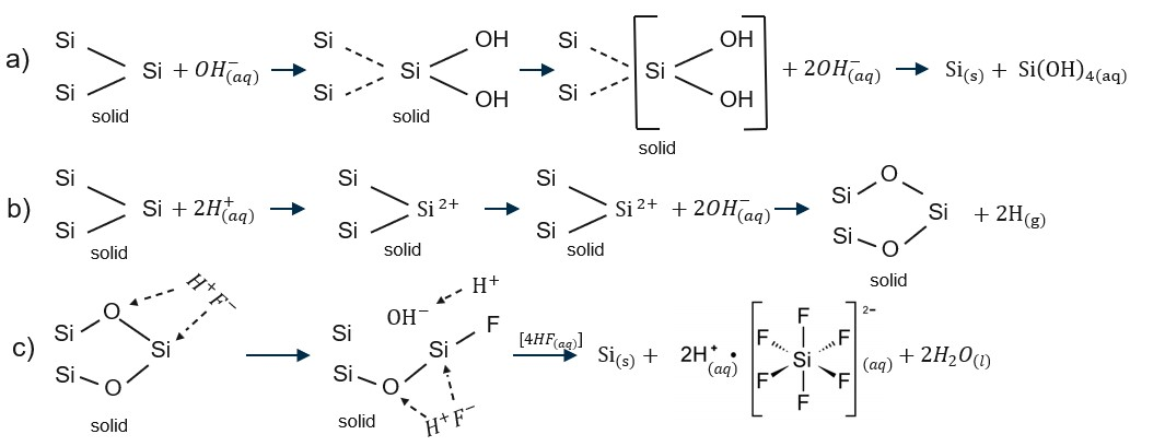
Silicon is wet etched by acids or alkaline solutions. In alkaline solution the surface atoms are terminated by hydroxyl groups which weakens the bonds to the bulk atoms below thus leaving surface silicon vulnerable to attack by the etchant. In acid etching the silicon is first injected with holes, after which it is oxidized by hydroxyl groups. Another acid that is able to etch silicon dioxide attacks the oxidized silicon atoms. Figure 5a shows how silicon is wet etched by alkaline solution and figure 5b how silicon is oxidized by acid such as nitric acid. Figure 5c shows how this silicon dioxide is wet etched by HF. The siloxane bridge is attacked first to form silanol species at the surface . Silicon inertness to fluorine based acids only applies to unbiased and non-illuminated silicon . The selectivity of HF between Si and SiO2 can not be explained by reaction energies due to them being exothermic . Fluorine bonds to silicon are strong and release substantial amount of energy when broken. Fluorinations of SiO2 and Si have activation energies of 0.72-0.77 and 1.22-1.56 eV, respectively . With sufficient promoting, fluorine is able to etch silicon as well. in 15a hydroxyl termination weakens the silicon bonds in to bulk that allows removal of surface silicon atom. In 15b protons inject holes into silicon atom that allows hydroxyl groups to attack nucleophilically and oxidize the silicon atom. In 15c HF performs electrophilic and nucleophilic attack simultaneously.

Figure 15: a) Alkaline etching of silicon b) Silicon oxidation by liquid acid c) Wet etching of silicon dioxide by HF
4 Conclusions
The main objective of this work was to study the potential for wet etching chemistry to reduce the sidewall roughness and improve the profile of vias etched by DRIE, understand the limitations for wet post-process modifications and ultimately determine if these process can improve via filling with copper. Vias of 5-25 µm diameter were fabricated using Bosch process, that were subsequently subjected to varying mixtures of HF/HNO3 with either acetic, phosphoric or sulphuric acid as additives. After this via post-process modification the vias were sputtered with copper seed layer and electroplated with copper. Wet etch impacts for empty and copper filled vias were characterized using optical and electronic microscopes. By qualitative evaluation on our results decreasing the roughness is expected to help with seed layer deposition while tapering the via seems to improve electroplating step. Tapering did not improve seed layer sputtering noticeably and certainly not to the extent that sputtering would reach the bottom of our via. As for roughness improvement method wet etching reached approximately 8-10 microns to the via in depth which makes it very limited whereas optmizing the DRIE recipe can produce vias that are smooth from top to bottom. Oxidizing the silicon and removing the oxide works efficiently as smoothening method but severely limits process option in terms of thermal budget since most metals used in electronics can not endure over 1000◦ C temperature such as aluminum, copper or gold.
Optimizing the HF/HNO3 mixture revealed significant diffusion related limitations for the process. Roughness reduction was hindered by insufficient flow and high boundary layer resistance in the deeper reaches of the vias. While profile modification were more successful, in this study it proved impossible to achieve optimal roughness reduction in likeness to smoooth etch regions of HNA and simultaneously optimal sidewall profile. The aggressiveness of the solutions would create steady taper yet diffusion was unable replenish the etchants at the bottom of the via efficiently enough to maintain high AR. Most of the etchants were consumed at the top which resulted in strong widening at the mouth while the bottom part remained almost untouched. However, while the bottom was relatively untouched etching did happen there.
下一篇: 异构集成InP-Si片上光子元件的优化