Inorganic micro light-emitting diodes (micro-LEDs) based on III-V compound semiconductors have been widely studied for self-emissive displays. From chips to applications, integration technology plays an indispensable role in micro-LED displays. For example, large-scale display relies on the integration of discrete device dies to achieve extended micro-LED array, and full color display requires integration of red, green, and blue micro-LED units on the same substrate. Moreover, the integration with transistors or complementary metal-oxide-semiconductor circuits are necessary to control and drive the micro-LED display system. In this review article, we summarized the 3 main integration technologies for micro-LED displays, which are called transfer integration, bonding integration, and growth integration. An overview of the characteristics of these 3 integration technologies is presented, while various strategies and challenges of integrated micro-LED display system are discussed.
Introduction
The concept of micro light-emitting diode (micro-LED) was put forward in 2000 , and extensive scientific research on microLED has been revitalizing the LED industry for more than 2 decades . Benefiting from the advantages of traditional LED, micro-LED display based on III-V compound semiconductors possesses higher efficiency, lower energy consumption than liquid crystal display, higher brightness, and longer lifetime than organic LED display. Therefore, micro-LED display has been considered as a promising candidate for the next-generation display technology . Unlike conventional large-area LEDs for lighting, micro-LEDs have typical pixel (micro-LED die) sizes below 100 μm or even 50 μm. Such a small size brings great challenges to the array arrangement and system integration of micro-LED displays. At present, integration technology has become the most critical problem in the development of high-performance micro-LED displays.
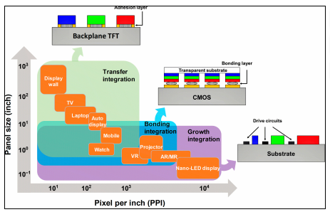
From the perspective of manufacturing process, the integration of micro-LED displays can be summarized into 3 categories: transfer integration, bonding integration, and growth integration. The transfer integration is integrating several discrete devices in a package with wire bonding or metal connects. In the micro-LED display technology, the transfer integration is used to assemble the micro-LED dies on the receiver substrate, followed by forming electrical interconnects. The bonding integration is a common heterogeneous integration in traditional semiconductor devices. Wafer bonding can be used for integrated devices or materials in the micro-LED display system . The so-called monolithic hybrid, which is achieved through a flip-chip process, can realize high-resolution matrixaddressable micro-LED display. The growth integration means that the materials making up the system are all grown on the same substrate. The integrated modules for micro-LED display go through a full monolithic process. Growth integration works for both homogeneous devices and heterogeneous devices in horizontal or vertical forms. Selective epi removal (SER) and selective area growth (SAG) are regarded as 2 feasible schemes for the growth integration of micro-LED displays. Different process conditions of above 3 integration technologies qualified their own structural characteristics and application tendencies. Figure 1 summarizes a series of micro-LED application scenarios, as well as their characteristic display area (panel size) and pixel density (pixel per inch [PPI]). The insets show schematic diagrams of micro-LED pixels prepared by 3 types of integrations mentioned above.

Fig. 1. The main application scenarios of micro-LED display and their characteristic display area and pixel density. The insets are corresponding schematic diagrams of microLED subpixels fabricated by transfer integration, bonding integration, and growth integration.
Over the past few years, many review papers about microLED have gradually emerged, which cover material preparation, device optimization, and application development of micro-LED. However, unrelated to the science of materials and devices, detailed review upon the integration technology was unique to the field of the science of micro-LED displays and yet lacking. In the following sections, we present an overview of transfer integration, bonding integration, and growth integration of micro-LED in turn. Finally, the micro-LED integration and its future development are summarized and prospected.
Substrate release of micro-LED array
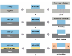
Commonly, GaN-based micro-LEDs are grown and fabricated on silicon or sapphire substrate and AlGaInP-based micro-LED on GaAs substrate. The grown substrates often have a thickness of hundreds of microns. Such a large thickness will bring trouble to the electrical interconnection and thermal management of the transferred micro-LEDs. Therefore, substrate release or removal is a prerequisite for almost all picking and transferring processes. Besides, the choice of substrate release techniques needs to take physical and chemical properties of corresponding material into consideration. Figure 2 shows common substrate release techniques used by different donor substrates. Generally speaking, the growth substrate of micro-LED can be released physically and chemically. The physical methods include laser lift-off (LLO) and mechanical grinding techniques. The chemical methods include acid or alkali wet etching.

Fig. 2. Schematic illustration of the processes of substrate release by (A) LLO, (B) mechanical grinding, and wet chemical etching using (C) alkali and (D) acid solutions.
Picking and placing of micro-LED
After substrate release, picking and placing were conducted. In this process, high transfer speed and high transfer precision are 2 key technical parameters to realize low-cost and highresolution display. Here, we mainly discussed elastomer stamp and laser selective release, which were proven to have outstanding transfer performance.
Summary and Outlook
According to the processing characteristics of micro-LED displays, we have defined 3 integration forms: transfer integration, bonding integration, and growth integration. For each integration form, typical research reports in recent years have been introduced and reviewed. Transfer integration has made great progress in fabricating large-area flat-panel display, while showing excellent potential in flexible wearable displays. With the yield increase and cost reduction of the mass transfer, transfer integration will greatly advance commercialization of microLED displays. Bonding integration has unique advantages in achieving high-resolution displays. With precisely aligned wafer bonding, monolithic hybrids of micro-LED array and CMOS driving circuit are expected to realize fully integrated programmable display systems, which benefits portable microdisplays. In addition, growth integration is hoped to achieve fully monolithic systems. With united material platform and process management, growth integration enables a more compact micro-LED display with high efficiency and low energy consumption. Merely, further development of growth integration in micro-LED display needs to address problems of full color and aperture ratio of subpixels. As a matter of fact, a truly practicable display requires the coordination of multiple integration techniques. In the whole system of micro-LED display, complete manufacturing often consists of transferring, bonding, and growing process of materials and devices.
上一篇: 异构集成InP-Si片上光子元件的优化