Abstract: Silicon carbide (SiC) is emerging rapidly in novel photonic applications thanks to its unique photonic properties facilitated by the advances of nanotechnologies such as nanofabrication and nanofilm transfer. This review paper will start with the introduction of exceptional optical properties of silicon carbide. Then, a key structure, i.e., silicon carbide on insulator stack (SiCOI), is discussed which lays solid fundament for tight light confinement and strong light-SiC interaction in high quality factor and low volume optical cavities. As examples, microring resonator, microdisk and photonic crystal cavities are summarized in terms of quality (Q) factor, volume and polytypes. A main challenge for SiC photonic application is complementary metal-oxide-semiconductor (CMOS) compatibility and low-loss material growth. The state-of-the-art SiC with different polytypes and growth methods are reviewed and a roadmap for the loss reduction is predicted for photonic applications. Combining the fact that SiC possesses many different color centers with the SiCOI platform, SiC is also deemed to be a very competitive platform for future quantum photonic integrated circuit applications. Its perspectives and potential impacts are included at the end of this review paper.
1. Introduction
Photonic integrated circuits (PIC), also named integrated lightwave circuits (ILC) or photonic lightwave circuits (PLC), have been discussed to overcome the predicted bottleneck for integrated circuits for more than half a century. During the development of PIC, a lot of different material platforms have been investigated, such as silicon (Si), silicon dioxide (SiO2), silicon nitride (SiN), aluminum gallium arsenide (AlGaAs), indium phosphide (InP), and the emerging gallium nitride (GaN), lithium niobate (LiNbO3), silicon carbide (SiC), etc. Although Si is playing the most important role in this area, benefiting from the well-established complementary metal-oxide-semiconductor (CMOS) processing, it is limited by its own optical properties, such as indirect bandgap, strong two-photon absorption at telecommunication wavelength and zero second-order nonlinearity. Therefore, other material platforms are developed either monolithically on their own or as hybrid platforms that are integrated with an Si substrate. Among them, SiC is emerging rapidly in this field, partially because of the commercially available high-quality crystal SiC wafers and mature micro and nanofabrication of SiC in the promotion of SiC powered electronic devices, a similar story as Si. Unlike many well defined figures of merit (FOM), such as Johnson FOM, Keyes FOM, Baliga FOM, and Baliga high-frequency FOM, for direct comparison of different material platforms in electronics, photonic material platforms are usually compared in terms of bandgap, refractive index, second-order nonlinearity, and third-order nonlinearity.
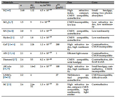
Normally, for an ideal PIC material platform, it has low loss at the working wavelength; has a high refractive index for strong light–matter interaction; has strong second-order nonlinearity for electro-optical modulation and second-harmonic generation; and has high third-order nonlinearity for efficient wavelength conversion. As shown in Table 1, SiC fulfills all the demanded optical properties: high refractive index, wide bandgap, and high second-order and third order nonlinearities. Additionally, SiC is CMOS compatible. Therefore, extensive investigations on SiC optical devices are emerging.

Table 1. Main material platforms for PICs. n: refractive index, BG: bandgap, n2: nonlinear refractive index, χ (2) : second-order susceptibility
2. Silicon Carbide Photonic Integrated Platforms
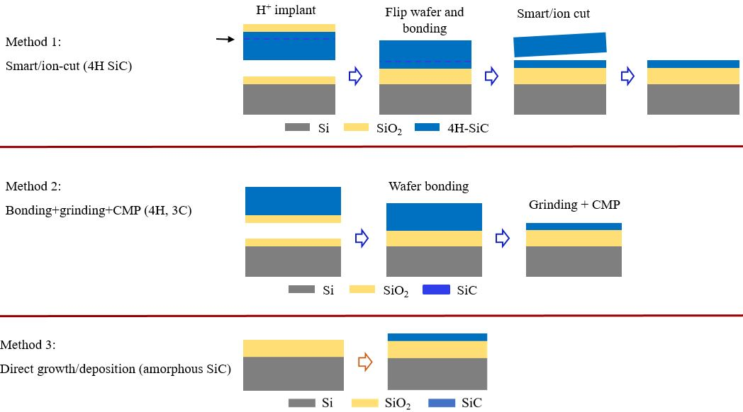
Planar optical waveguides are key structures where the light is confined and transmitted by obeying total internal reflection (TIR). For SiC waveguides, it is indispensable to form an index contrast where SiC has a higher refractive index than the surroundings. At the beginning of this research, floating SiC in the air has been applied because the commercial SiC epilayers on Si substrates were available. Since Si has a higher refractive index than SiC, it has to be removed near the SiC waveguides. But this structure has restrictions on the post-etching process, such as patterning and top-cladding deposition. Instead, silicon carbide on insulator stacks is developed and applied in most of the publications currently. There are generally three different methods to form SiCOI, as shown in Figure 1. For method 1, smart/ion cut method is adopted from silicon-on-insulator (SOI) stack’s formation, where Si wafer is replaced by a SiC wafer . But since SiC and Si have very different physical properties, the material loss in SiCOI is still quite high compared to SOI, after ion implantation. This method mainly delivers 4H SiCOI stacks. For method 2, the bonded SiC is thinned down directly by using grinding and later chemical mechanical polishing (CMP) to smoothen the surface. In this way, the ion implantation step in the smart/ion cut is skipped and SiCOI stacks achieve very low loss. This method delivers 4H and 3C SiCOI stacks. For method 3, amorphous SiC is directly deposited on the Si substrate with an SiO2 layer between. The amorphous SiC deposition could be completed through plasma-enhanced chemical vapor deposition (PECVD) and sputtering. Both methods are CMOS compatible.

Figure 1. Three SiCOI stack formation methods.
3. Silicon Carbide Photonic Cavities
3.1. Microring and Microdisk Resonators
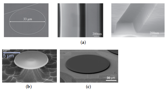
Thanks to the advanced nanofabrication technologies, SiC microresonators, including MRR and MDR, with low loss and high quality factors, have been demonstrated. The loss is jointly contributed by the material absorption loss and the light scattering loss due to the surface roughness. Figure2 shows scanning electron microscope (SEM) images of several high-performance SiC microresonators.

Figure 3. Scanning electron microscope images of (a) 4H SiCOI MMR, reprinted with permission from ©The Optical Society, (b) 3C SiC MDR , and (c) 4H SiCOI MDR .
For 3C SiC, using the freestanding SiC, grown on the Si substrate, quality factors of 2.4 × 10⁴and 5.12 × 10⁴ have been reported for MRR and MDR, respectively. The high loss mainly comes from the material absorption and is associated to the high density of extended defects, inherently linked to the 3C-SiC/Si heteroepitaxial system, and discussed in the coming section. The highly defective layer, which is close to the 3C-SiC/Si interface, can be removed, if preparing 3C SiCOI stacks. As a result, microresonators with much higher quality factors can be achieved, which are 1.42 × 10⁵and 2.42 × 10⁵, for MRR and MDR, respectively. For 4H SiC thin film prepared through the smart/ion cut method, quality factors of 7.3 × 10⁴and 5.25 × 10³ have been reported for MRR and MDR, respectively. Chemical-mechanical polishing and post-oxidation processes can also help to reduce the roughness of the top surface and the sidewall of the waveguides, and thus improve the quality factors of SiC microresonators, for both 3C and 4H SiC . For 4H SiC thin film prepared through the grinding and CMP method, ultra-high quality factors of 1.1 × 10⁶ and 6.75 × 10⁶ have been reported for MRR and MDR, respectively . Regarding the amorphous SiC deposited by PECVD, the MRR with a quality factor as high as 1.6 × 10⁵ has been reported. Based on these demonstrations of high-performance SiC microresonators, as well as other SiC integrated devices, SiC integrated platforms can be potentially applied to classical and nonclassical optical communication systems for signal processing, logic gate, modulation, filtering, (de)multiplexing, etc.
4. Impacts of Novel Photonic Applications of SiC
The research in silicon carbide started to have strong momentum in the 1990s. That decade had a heavy focus in research and in Europe several EU projects were initiated. The first ones were mainly in bulk growth and included some epitaxy and device development. Epitaxy and device challenges were heavily related to defects in research-grade wafers, and epitaxy recipes and issues such as stable electrical contacts were not in place. Test devices suffered from structural variations within wafer areas, as well as between wafers. The first European wafer suppliers emerged 20–25 years ago and slowly substrates became more available for device development. The market started to grow slowly, firstly by the sale of materials. It was only when devices became available that the market started to grow faster. The SiC diodes and power electronics pushed the market, and also started to require more wafers. As a consequence, the wafer prices have steadily decreased and volume manufacturing is now established. Today, many market players are entering and the SiC device market will grow to billions of US dollars annually. The journey from research to a strong, growing SiC market has taken about 30 years.
上一篇: 碳化硅化学机械抛光技术最新进展