Abstract
This paper considers the nature and value of the information contained in the distribution of good circuits across production IC wafers. It is shown that the actual production wafers are perhaps the only source of information available at rea- sonable effort and cost which reliably reflects the true yield -limiting factors existing in the process. Communication with these factors can be aided by analyzing the shape and orientation of the regions of the wafer wherein zero yield is obtained-thus, yield -area analysis. Fundamental divisions are made between parametric and point -defect limited yield. The key factor that allows the separation of these types is the quasi continuity of parametric values across wafers. It is suggested that any yield formula that assumes that point defects are the dominant yield -limiting factor must be multiplied by an area usage factor (AUF) which reflects the total fraction of available area being used for nonzero yield. On many wafers the AUF is less than 02, thereby making it one of the most important characteristic parameters of the process.
1. Introduction
During the course of manufacturing integrated circuits one finds many opportunities for destroying potentially good circuits on a wafer. These opportunities fall into three basic classes (1) ignorance, (2) neglect, and (3) inability to prevent. It is primarily with regard to the first class that this paper is addressed. If one knows that certain problems exist, then diagnostic efforts are redundant. If one does not exercise effective controls then he deserves the consequences of an uncontrolled process. On the other hand, if one is doing his best to control his process, it is essential that he understand how to analyse all important available sources of information concerning the nature of the causes for nonworking circuits. One rich, yet frequently overlooked, source of information is the distribution of working circuits over the wafer. This paper attempts to provide a foundation for analysing these distributions and to suggest the causes of the nonideal dístríbutíons frequently observed on production wafers used for LSI circuits.
2. Preliminary Discussion
2.1 Point Defects versus Parametric Defects
When one has obtained a sizable set of wafer maps of working circuits from individual wafers produced from the process of interest he has the basic starting data. These maps may be obtained by any of several means as discussed later in this paper. If any circuits at all on a wafer work, one must assume that the gross features of the process were performed satisfactorily. Those wafers that have no working circuits may or may not have had gross processing mistakes. In any case, since no working circuits exist there is no data and these zero yield wafers will be ignored for the purposes of this paper. The failure of the non -working circuits to satisfy the testing criteria must have been caused by parametric variations that were incompatible with the circuit design or by local physical disruptions (commonly called point defects). Chemical nonuniformities may also exist but these will be reflected in an electrical or physical property and do not need to be directly considered. These causes for failure assume that the testing process itself reliably indicates working and nonworking circuits and does not suffer from mechanical problems, such as probing or electrical problems (for example, noise or transients).
3. Experimental
3.1 Data Collection
Except in special cases where a dominant problem exists that is easily visible (such as metal damage for example), the only data routinely available that is suitable for addressing the question of processing problems and for determining the real yield -limiting factors is the data exístíng from the electrical testing of the actual circuits of interest.
There are several reasons why the use of production wafers as the source of data ís good (and is much better than attempting to use artifacts that are sensitive to only a small part of the total process). The main reason for using the circuit itself for the diagnostic tool is that it represents the actual item of primary interest. It contains the primary data.All the idiosyncracies that might cause a problem are present in the exact form of interest, namely in the circuit itself. A second, very important, reason for using the circuit, if possible, is that a semi -continuous sampling of the actual behavior of the production line is available. This is virtually impossible to obtain from any non -salable artifact, primarily because of the high cost of processing and testing and general unwillingness to commit production resources for this kind of work.
3.2 Results
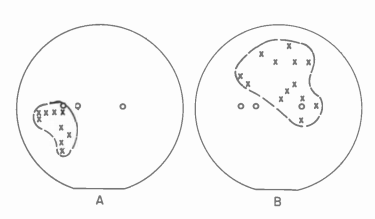
Fig. 1 shows data from three different lots of SOS/CMOS 1K RAM's processed on 3 -inch sapphire wafers. The X's indicate the position of the good circuits and the 0's indicate the "knock out" positions. Cursory inspection reveals that self -consistency within the same wafer exists within the nonzero yield areas. For these wafers, particularly F, G, H and K, one can identify multiple regions of nonzero yield. The local yield varies strongly from wafer to wafer, thus indicating the unpredictability of effective defect densities even under nominally identical conditions. The most important observation to make, however, is the vast areas of zero yield that exist on most of the wafers. Good circuits are obtained within two or three pellet spacings of the wafer edge on many of the wafers. This clearly defines the handling distance to be on the extreme outer portions of the wafer. For this set of data, parametric incompatibility probably accounts for the major part of the bad circuits. If this process and circuit design were compatible in a parametric sense, the overall yield would be at least tripled.


Fig. 1-Yield distribution from three typical lots of SOS 1K RAM parts. The lightly dashed lines in F, G, H, I, and K indicate alternate choices for the loci.
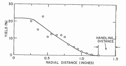
It is worth noting at this point that plots of radial distribution of yield (such as shown in Fig. 2 for data similar to that of Fig. 1) will nearly always show a dramatic falloff in yield as one proceeds away from the center of the wafer. These plots primarily reflect the nonuniform use of area rather than radial distributions of local yield. Inspection of the actual distributions shows that local yields are quite high near the edges for many of the wafers. Therefore, while radial distribution plots are useful for demonstrating the the poor usage of the outer areas of the wafer, they are not suitable for diagnostic work. Furthermore, the slope of the radial distribution curve indicates that gradual transitions exist between high- and low -yield areas of the wafer. Inspection of the actual maps show this to be completely untrue.

Fig. 2-A typical plot of the radial distribution of yield from data similar to that of Fig. 1.
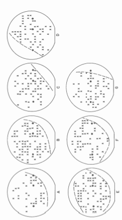
For the particular case of the SOS RAM data of Fig. 1, reasonable test devices existed on the circuit periphery for acquisition of electrical data. Examination of these devices across entire wafers showed that none of the measured electrical parameters were incompatible with the circuit design. Visual inspection, however, revealed that a good chance existed that the physical tolerances required for the circuit were too demanding for the available technology. An effort to make the circuit more compatible with the process by making only the physical tolerances of the circuits less demanding (not the design or testing procedure) produced dramatic increases in the total fraction of the wafer that produced working circuits. This data is shown in Fig. 3. The major difference between the data of Fig. 3 and that of Fig. 1 is that much more of the non - edge region is used for yield. The local yield on some of the wafers of Fig. 1 is as high as that for most of the wafers of Fig. 3. We can therefore conclude that the increase of wafer area used for yield (AUF) was a direct result of less critical physical tolerances being required.

FIG3
4. Discussion
The data in the preceding section amply demonstrates that large yield loss can and does occur for reasons other than isolated point defects. Clustering of good circuits can be caused entirely by parametric incompatibility. Multiple, well developed clusters of good circuits were never found, although some wafers showed some clustering of low yield and a very few had some multiple nonzero yield regions. These low -yield clusters could be caused either by defects or by parametric problems. If lack of defects caused the high -yield clusters, why were only single, well developed clusters (which usually occur near the alignment keys) found on the same wafer.
5. Conclusions
The data and discussions in this paper have led to the following conclusions: (1) The primary conclusion is that significant information concerning the processing of wafers is contained in the distribution of good and bad circuits across production wafers and that this data is available with minimal acquisition effort. (2) Application of yield models which assume that defects are the dominating influence must be restricted to the nonzero -yield portions of the wafer. The result of these models must be multiplied by the appropriate area usage factor (AUF) to arrive at the proper result. (3) Great value in terms of better circuit design and yield can be expected by understanding the parametric properties of whole wafers and using these results to direct process improvement efforts precisely where they belong. (4) Examination of several lots of actual production wafers has clearly shown the existance of large areas of zero yield with most wafers exhibiting sharp dividing lines between zero- and nonzero -yield areas. (5) Within the nonzero -yield areas of the same wafer, reasonable uniformity of local yield exists. (6) The local yield varies widely from wafer to wafer and therefore is essentially a priori unpredictable for individual wafers. (7) In many cases the areas of zero yield are caused by parametric incompatibility-not by defects. (8) Actual production circuits are one of the best tools for defect related yield studies. Artifacts cannot be processed with the volume required for determining the true effects of the total process without gross expenditure of possibly uncompensated money and effort. (9) Plots of radial yield distribution are very likely to be misleading in terms of the sharpness of the transistion between the zero- and nonzero -yield portions of the wafer. Only the original map is truly suitable for detailed examination. (10) For parametric diagnostic purposes it is important to consider individual wafers as opposed to statistical collections. Statistical collections can produce some information concerning constantly failing sites (mask defects) or gross population shifts, but they mask the true shape of the yield loci in much the same way as radial distribution plots.
上一篇: 氮化硅表面的蚀刻和化学控制
下一篇: 硅的湿法化学刻蚀机理