ABSTRACT
We review what can be said on wet chemical etching of single crystals from the viewpoint of the science of crystal growth. Starting point is that there are smooth and rough crystal surfaces. The kinetics of smooth faces is controlled by a nucleation barrier that is absent on rough faces. The latter therefore etch faster by orders of magnitude. The analysis of the diamond crystal structure reveals that the { 11 1) face is the only smooth face in this lattice - other faces might be smooth only because of surface reconstruction. In this way we explain the minimum of the etchrate in KOH:H20 in the <001> direction. Two critical predictions concerning the shape of the minimum of the etchrate close to <001> and the transition from isotropic to anisotropic etching in HFHN03 based solutions are tested experimentally. The results are in agreement with the theory.
I. INTRODUCTION
Anisotropic wet chemical etching of single crystalline silicon, gallium arsenide and quartz is one of the key technologies for the fabrication of microsystems. Yet the strong anisotropy of the etchrate in particular etching solutions (e.g. KOH:H20, EDP, TMAH), and the isotropy in others (e.g. HFHN03:HzO) is poorly understood. Mostly the anisotropy of the etchrate is related to chemical reactions on the crystal surface oriented in different crystallographic directions. In this respect maybe the most advanced picture has been proposed by Seidel et al. 111. They assumed that the complex formed by the attachment of an OH-ion to the dangling bond, after the electron has been delivered to the solid state, changes the back-bond energy of the silicon atom with three back-bonds in a different way than iin the situation when one has two OH attached to the silicon atom with two back-bonds. The difficult point however is that the silicon atoms have three backbonds also in the flat face, not only in the flat face; therefore, etchrate and activation energy in these crystallographic directions should be comparable in contrast to experimental evidence.
In this paper we add a number of new experimental results which support the view given here. In particular, we have looked with greater detail at the dependency of the etchrate of silicon etched in KOH on the crystallographic orientation close to the <loo> direction, and we studied the transition to anisotropic silicon etching in HFHN03:CH3COOH.
11. THEORY
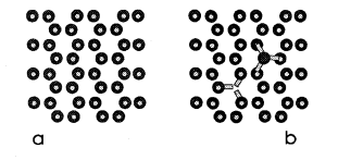
In kinetics of crystal growth active sites for growth and dissolution play a key role. These active sites are atoms with as many bonds to the crystal as to the liquid (or gaseous) environment. Such a site is called a kink site. An atom in a kink site in a simple cubic lattice is shown in fig. la. The heavy shaded atom has three bonds to the crystal and three bonds to the liquid. In a dissolution situation it is commonly believed that this atom will diffuse over the surface (fig. lb), until it either finds a kink position again or it desorps and diffuses away from the crystal in the liquid phase (indicated in fig. IC). In a growth situation, an atom diffuses from the liquid to the crystal (fig. IC), it diffuses over the crystal surface (fig. 1.b) until it is either desorped or it finds a kink site (fig. la).

Fig. 1 Illustration of kink sites and the elementary kinetic processes for etching @om a to c) and for growing from c to a) crystak
Kinetic rates (for growth and dissolution) thus depend critically on the number of kink sites on a crystal surface. This aspect was neglected so far in the discussion of etch rates of single crystals such as silicon, quartz and GaAs. Only parts of the total process have been considered: the chemical reaction rate (which is important for the adsorption process and the kink integration process, erroneously considered anisotropic), diffusion in the liquid solution (isotropic), and the thickness of the boundary layer. In our view, the most prominent anisotropy effect is due to the number of kink sites.
Consider the energy difference of the two situations depicted in fig. 2. In fig. 2.a we show the (111) silicon surface as one obtains by simply cutting the crystal along the (111) plane. The dangling bonds are indicated by light dots. In fig. 2.b we have cut one atom out of the surface and placed it back somewhere else on the crystal surface. To do this one has to cut three bonds of strength + each, but one bond is delivered by placing back the atom onto the surface. The energy difference △E = 2Φ.

Fig. 2 Energy required to create a cavity-adatompair on an unreconstructed {lll) face of the diamond lattice. △E = 2Φ
This is very much diffeent from the {00l) silicon face as can be seen in fig. 3. The same operation - creating an adatom-cavity pair - now costs no energy, because one has to break two bonds in order to remove an atom from the (001) face, but one gets them back by placing it back to any position on this face.

Fig. 3 EnergV required to create a cavity-adatom pair on an unreconslructed {OOll face in the diamond lattice. △E = 0
The energy difference AE divided by kT (absolute temperature times Boltzmann constant) is known as the a-factor of Jackson (see, e.g. 131) and plays a key role in theory of crystal growth. At sufficiently low temperature kTa is proportional to the step free energy y. The essential difference between the (111) and the (001) silicon face is: In equilibrium the { 111) face is smooth at sufficiently small temperature and the (001) is rough. The step free energy y is finite of the { 11 1 } , and zero of the (001) face of silicon. The number of cavity - adatom pairs is proportional to exp -a. This number is very small on the (111) silicon face at low temperature, but 1 on the (001) silicon face at any temperature.
111. EXPERIMENTS
111.1. Anisotropic etching From (iv) of section I1 it follows that the etchrate E and growth rate G vary proportional to the absolute value of the angle of misorientation. In agreement with experimental results, see fig.4. Similar results have been published by Kendall. However, the situation close to the <l00> directions is unclear. In the <l00> - direction there is also a minimum if one etches silicon in KOH and NaOH. In situations where the minimum is steep enough it is possible to micromachine vertical <l00> walls in <001> oriented wafers. Mirror like flat {l00)-faces have been reported at particular etching conditions (35 wt% KOH, 80 "C). Possibly the (100) are flat under these conditions in which case eq. (1) would apply.

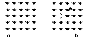
Fk. 4. A screw dislocation gives rise to a step on the crystal surface (a). The step moves when the crystalgrows (b) and if it is etched (c)
IV. DISCUSSION
The minimum of the etch rate at the <l00> direction implies in our view that the {l00} faces are flat when they are in contact with KOH solutions investigated in our experiments. This is only possible if the surfaces are either reconstructed or if there is an adsorption layer on the {l00} faces that stabilise in some way the surface . To our best knowledge, this is the first time that some evidence of surface reconstruction of silicon surfaces in contact with an etching solution is given. Certainly, the step free energy on {l00} is considerably smaller than on the I1111 faces, as evidenced by the large etch rate of the {l00}. This is consistent with the absence of high steps on slightly disoriented {l00} faces. These high steps are created by "collisions" of steps, a process that is strongly enhanced by adsorption of impurities at the surface .
上一篇: 硅、锗、砷化镓和磷化镓的化学蚀刻