A comprehensive review of dynamics of etching and its various applications in silicon wafer processing is accomplished, and new developments are discussed. A previously proposed pseudo two-phase phenomenological model to describe the dynamics of three-phase etching is revisited and novel augmentations are proposed. Interplay between the liquid-phase transport of reagents, the silicon surface kinetics, and the formation and the transport of gaseous bubbles is quantified. Both the model and the reported data explain effects of etching on silicon-surface polishing. Recent attempts to extend the pseudo two-phase model to describe the defect decoration by acidbased etching are discussed and new modifications are proposed. Microdefect (agglomerated defect) distribution in a monocrystalline silicon wafer is identified by growing copper precipitates on the microdefects followed by surface polishing and subsequent microdefect-decorating etching, which forms the pits on the wafer known as etch-pits by a relatively rapid chemical dissolution of the precipitates. The macrodecoration of microdefects is typically realized in the absence of significant effects of the liquid-phase mass-transport. The developed phenomenological model leads to classification of etchants as either polishing or potentially decorating and to the identification of conditions necessary for an efficient microdefect decoration. The reported analytical expressions for the microdefect-decorating and the microdefect-polishing conditions are also revisited, revised, and augmented. A series of reported experiments validates the developed model.
Introduction
Acid-based etching is widely applied in the manufacture of monocrystalline silicon substrate for device fabrication. Two important applications of etching are in the surface polishing of silicon wafers to remove mechanical damage and in the characterization of the microdefects that play a critical role in device failure. In this paper, a review of the reported developments in acid-based etching is presented. Recent developments in the quantification of quality of the surface polishing and the microdefect characterization (also known as decoration) are extensively discussed, and further revisions and modifications to the published models are proposed. Thus, this paper revisits and reviews the relevant literature in the field of acid-based etching and proposes new developments based on the unpublished research of the author of this paper.
Section I: Acid-Based Etching in Surface Polishing
Semiconductor silicon substrate wafers are prepared through various chemical and mechanical processes. First, silicon single-crystal ingots are sliced into circular disks by slicing followed by a flattening process called lapping that involves scrubbing the sliced wafers using an abrasive slurry.1 Acid-based etching, which is the focus of this paper, removes the mechanical damage induced during the previous shaping processes and chemically polishes the wafer surface. Various unit operations such as polishing and cleaning follow the etching before a wafer is ready for device fabrication.
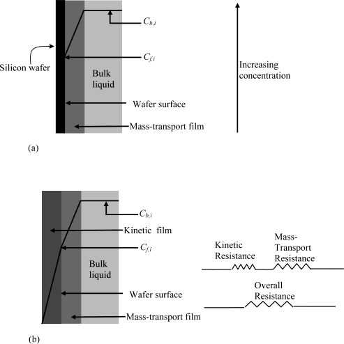
Two-Phase System: Quantification of Process Time Scales. Chemical etching of silicon wafers is a three-phase system that involves the liquid-phase trans port of reactants from the bulk liquid to the wafer surface, the surface reactions that generate products in both the liquid-phase and eventually the gas-phase, and subsequent transport of products into the bulk liquid.30 For the sake of simplicity, first, effects of eventual gaseous products on the surface morphology are neglected and a simple two-phase solid-liquid reaction system is treated (Figure 1a). The etching dynamics involving the formation of the gaseous bubbles is treated later in this study. In a two-phase system, according to the classical film-transport theory, the transport of reagents occurs by molecular diffusion through a liquid film, known as the concentration boundary layer or the mass-transport film, on the wafer surface.

Figure 1. Phenomenological representation of the two-phase etching system depicting (a) the mass-transport resistance and (b) the kinetic and the mass-transport resistances.
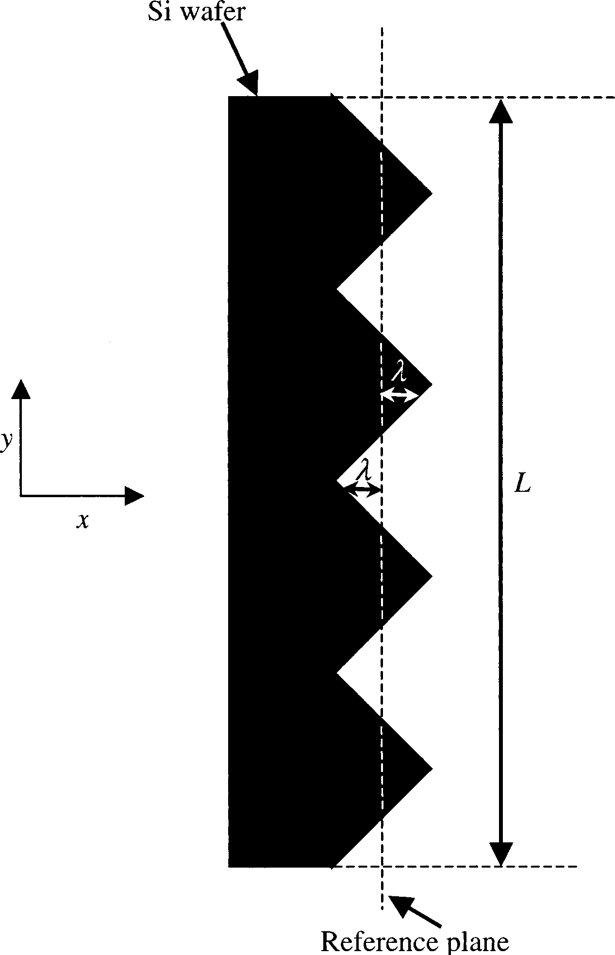
Application of the Resistances and the Quantification of Surface Polishing. One goal of etching is to reduce the surface roughness of wafers. The roughness is a measure of nonuniformity of the surface represented as a field of peaks and valleys (or troughs) (Figure 2).

Figure 2. Schematic representation of the roughness. Note that λ is the local distance between any location on the wafer surface, not just the lowest and the highest locations, and the mean reference plane (line).
Analysis of Surface Polishing.
Equation 11 describes the generic effect of the mass-transport and the surface kinetics in any etching process. Insight into the role of the transport on surface polishing, however, is better achieved by analyzing three limiting cases, each representing a popular industrial practice for varying the polishing efficiency. The following discussion describes a typical etching system following a reasonably real kinetics, although it can be extended to any generic case. Henceforward, the terms mass-transport and transport are used interchangeably to mean the same phenomenon.
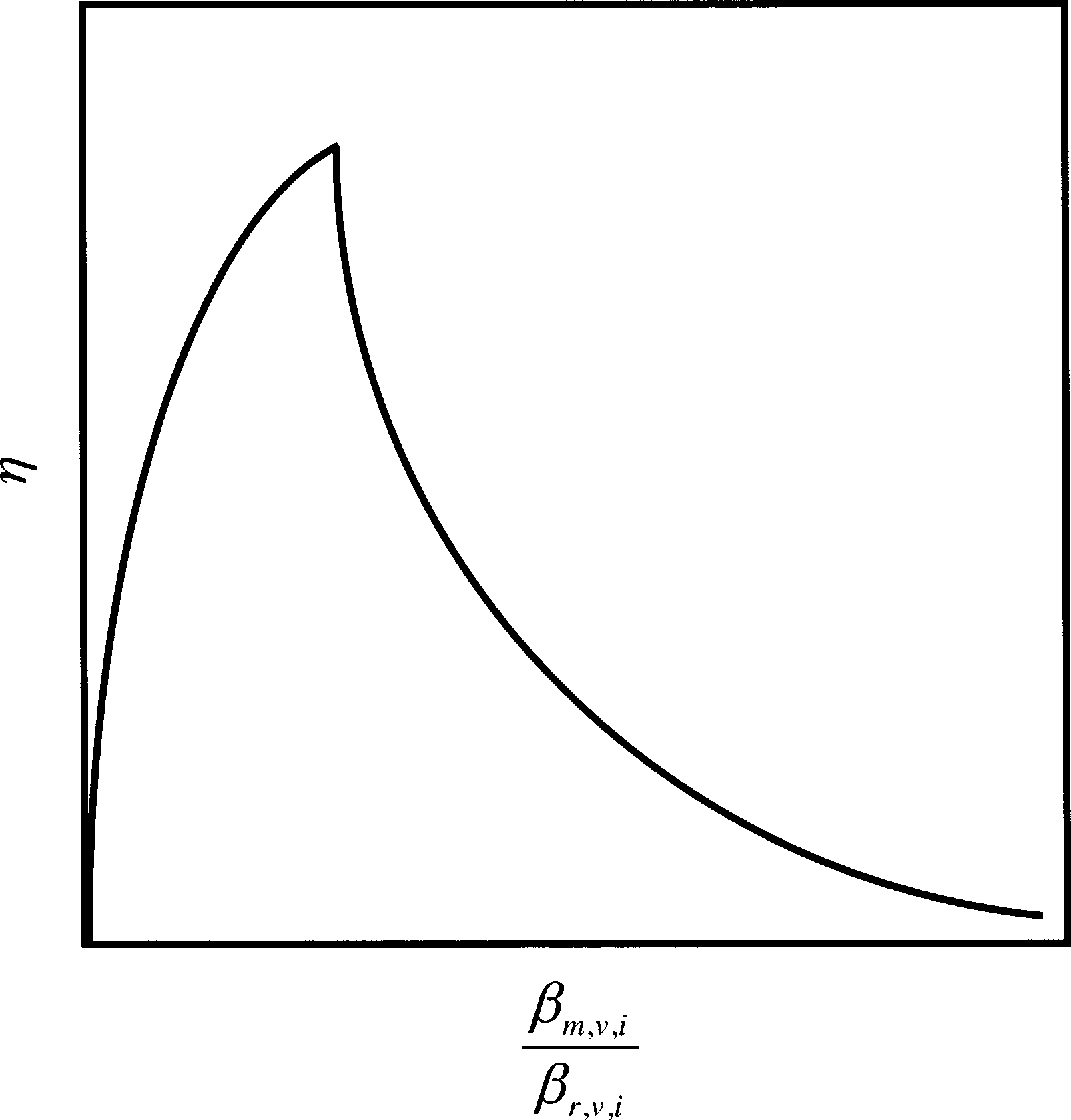
Figure 3 shows a typical qualitative dependence of the polishing efficiency on the ratio of the mass-transport resistance to the kinetic resistance. It must be noted that as this ratio changes, the kinetic resistance at peaks and that at valleys can also change. It is clearly shown here that the quality of surface polishing is a strong function of the interplay between the mass-transport and the surface kinetics. The desired etching conditions must be determined on the basis of this relationship.

Figure3. Typical dependence of the surface-polishing efficiency on the interplay between the mass-transport and the surface kineticssthe case of varying mass-transport film thickness.
Conclusions:
Acid-based wet (liquid) etching is popularly applied in the manufacture of monocrystalline silicon substrate for device fabrication. Two key areas of its application are chemical surface polishing, to remove prior mechanical damage, and defect decoration. A unifying pseudo two-phase model built on the basis of a complex threephase dynamics describes various aspects of the surface polishing and the defect decoration. At any given site on a silicon surface, various products of the etching reactions can form gaseous bubbles, which mask the site from further etching until they are dislodged into the liquid near the surface, through which the transport of reactants and products occurs. The masked site can form a peak if sufficient etching takes place on the surrounding unmasked sites. At a global level, the intense bubble masking leads to global surface irregularities. The entire three-phase dynamics can be represented by an equivalent etching system involving an effective reaction front on the wafer surface, to and from which the transport of reagents takes place through an effective mass-transport film in the liquidphase. Both the molecular diffusion and the dispersion induced by the dislodged bubbles contribute to the transport through the effective mass-transport film.
上一篇: 硅的湿法化学刻蚀机理