The fabrication of hybrid materials consisting of nanoporous hosts with conductive polymers is a challenging task, since the extreme spatial confinement often conflicts with the stringent physico-chemical requirements for polymerization of organic constituents. Here, several low-threshold and scalable synthesis routes for such hybrids are presented. First, the electrochemical synthesis of composites based on mesoporous silicon (pore size of 7 nm) and the polymers PANI, PPy and PEDOT is discussed and validated by scanning electron microscopy (SEM) and energy-dispersive X-ray spectroscopy (EDX). Polymer filling degrees of ≥ 74 % are achieved. Second, the production of PEDOT/pSi hybrids, based on the solid-state polymerization (SSP) of DBEDOT to PEDOT is shown. The resulting amorphous structure of the nanopore-embedded PEDOT is investigated via in-situ synchrotron-based X-ray scattering. In addition, a twofold increase in the electrical conductivity of the hybrid compared to the porous silicon host is shown, making this system particularly promising for thermoelectric applications.
INTRODUCTION
Since the first publications on the remarkable properties of mesoporous silicon a lot of applications have been developed based on this material. Mesoporous silicon is used in photonics, opto-fluidics, gas-sensing, biomedicine, energy conversion, electromechanical actuation and as an anode material in batteries. It can also be used as a hard nanoporous scaffold for the study of confinement effects on the structure and dynamics of soft condensed matter systems. Conductive polymers in itself are also an enabling material class due to their general low cost and accessibility as well as their unique chemical and mechanical properties resulting in a plethora of different applications.
MATERIALS AND METHODS
Mesoporous silicon fabrication
Mesoporous silicon is produced by an electrochemical etching procedure based on the anodic silicon dissolution in hydrofluoric acids. The etching solution consists of a volumetric mixture of 3:2 HF (48 %) to Ethanol (EtOH, 99 %). A platin mesh works as the counter electrode (CE), the working electrodes (WE) are boron doped p+ wafers <100> with a resistivity of 0.01 to 0.02 Ωcm and a thickness of 525 µm. The samples used in the eltectrochemical polyermization procedures are etched at a current density of 12.5 mAcm−2 for 720 s, resulting in a mesoporous silicon layer with the long pore axis normal to the sample surface. The pSi layer is still attached to the underlying bulk silicon - hereinafter referred to as an epilayer (see Fig.2). The samples prepared for the hybrid fabrication based on the SSP, as well as the subsequent X-ray diffraction (XRD) measurements at DESY, were prepared in a different way. The used substrates are 100 µm thick, double side polished p+ wafers, with the same dopant, resistivity and orientation as the thicker wafers described before, meaning the anodic electrochemical dissolution and resulting mesoporous layer structure stays similar. The wafers were etched from both sides for 3200 s (at 12.5 mAcm−2 ) creating a sandwich structure (see Fig. 5). Naturally this is a two-step process. After each etching step every sample is cleaned in deionized water, ethanol and dried. This preparation route was necessary to ensure that a maximum pore space could be used without significant bending of the hybrid samples. Free standing membranes (detached from the underlying bulk Si) tend to crack during the recrystallization of the DBEDOT monomer after infiltration, meanwhile epilayers bend.
RESULTS
Mesoporous silicon
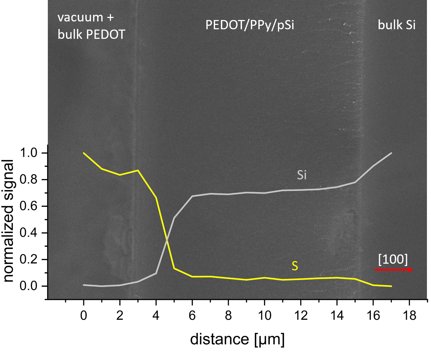
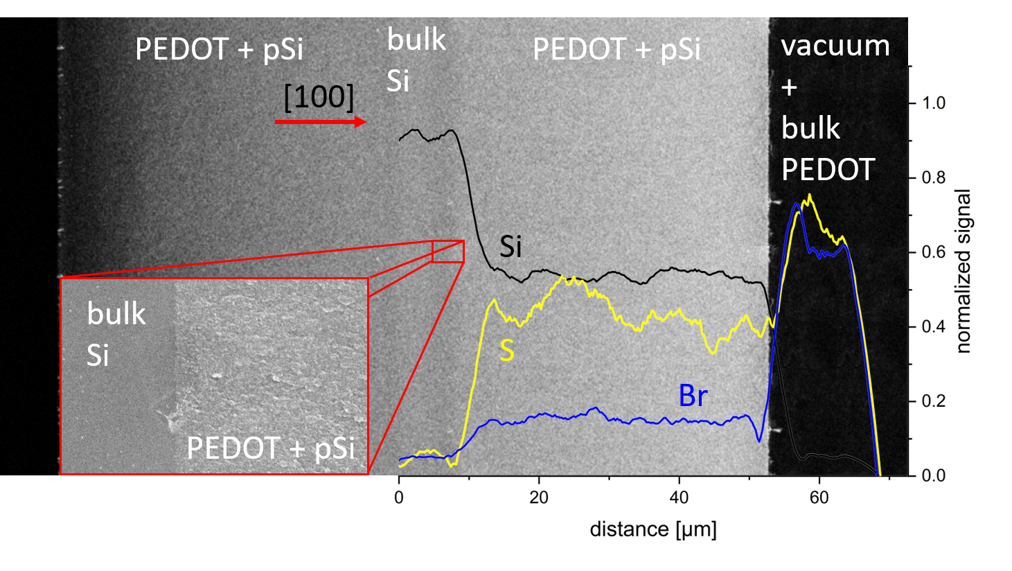
The anodic electrochemical etching of p+ silicon is a wellestablished procedure. For the given dopant concentration, current density and electrolyte composition the resulting average pore size is around 8 nm – 9 nm in diameter. The epilayer thickness of the pSi after anodic etching of the silicon for 720 s is 11.4 ± 0.2 µm (see Fig. 2). Combined with weight-loss of 9.02 ± 0.01 mg the calculated porosity is 43.2 ± 1.4 % inside the pSi layer, which matches well with literature data. The etching of the pSi/bulk Si/pSi sandwich structure, etched from both sides for 3200 s, results in the following layer thicknesses pSi = 45.8 ± 0.5 µm and bulk Si 11.6 ± 0.2 µm (Fig. 5). In the inset of Fig. 5 a close up of the dead-end pores is shown. The remaining bulk silicon is thick enough for uninhibited current flow, leading to a sandwich structure of constant thicknesses along the whole sample size (diameter of 3.16 cm). The measured porosity inside the first pSi layers is 50.3 ± 1.3 %, the porosity in the second 53.1 ± 1.3 %. The increase in porosity from 43 % to 50 % with increasing etching time is to be expected, due to chemical etching, diffusion processes and changes in HF concentration involved during the anodic etching of silicon.

FIG. 2. SEM micrograph and superimposed silicon (grey) and sulfur (yellow) EDX signal as a funcion of distance. In the middle part the 11.4 ± 0.2 µm thick mesoporous silicon (pSi) – filled with PPy and PEDOT is shown. The hybrid is attached to the underlying bulk Si (right site). In interest for greater clearity the EDX data for carbon, nitrogen and chloride are not shown. The red arrow indicates the crystal orientation as well as the pore axis perpenticular to the sample surface.

FIG. 5. SEM micrograph and superimposed silicon (black), sulfur (yellow) and bromine (blue) EDX signal as a funcion of distance. In the middle part the 11.6 ± 0.2 µm bulk Si layer is visible, left and right the 45.8 ± 0.5 µm thick pSi layer filled with PEDOT. The close-up shows an interface (dead-end pores) between the pSi and bulk Silicon.
Electrochemical polymerization of PEDOT/PPy/pSi hybrids
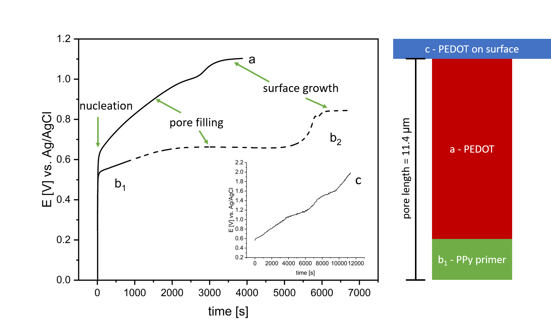
To the best of our knowledge, this will be the first time, that direct electrochemical polyermization of PEDOT in mesoporous silicon pore space is shown. It shall be briefly mentioned that the galvanostatic deposition method on active surfaces is typically favoured compared to potentiostatic methods. This is because the necessary potential for the oxidation of the monomer and subsequent polymerization is minimized, lowering site reactions and especially the oxidation of the pSi. As mentioned in the introduction, the direct electropolymerization in mesoporous silicon pore space is established for polybithiophen and PPy. Thus the expected curve shape during galvanosatic deposition is known from literature. The latter one is regulary used for the production of PPy/pSi hybrids and is shown in Fig.1b2. Throughout the deposition process, there is a gradual rise in the initial voltage, reaching up to 0.5 V. This increase is associated with nucleation occurring at the bottoms of the pores and the partial oxidation of the pSi. The ensuing potential plateau is explained by the ongoing deposition of PPy inside the mesoporous silicon matrix. After around 6000 s the epilayer is completely filled and the PPy begins to polymerize at the surface. The observable increase in potential (up to 0.8 V) is ascribed to the uninhibited growth and branching of the polymer at the surface, leading to an increase in electrical resistance if compared to the directional grow inside the pSi . In the inset of Fig.1c the galvanostatic deposition of PEDOT on an epilayer is shown. At around 0.6 V the oxidation potential of EDOT is reached and the electropolymerization readily proceeds. Compared to the PPy deposition in Fig.1b2, the characteristic transition regimes are missing and the voltage increases linearly with time.

FIG. 1. Voltage-time (E-t) transients during galvanostatic deposition of: a PEDOT in pSi-epilayer on a 2 µm PPy primer layer, b1 2 µm PPy primer layer (for 878 s), b2 complete filling of the epilayer with PPy and c deposition of PEDOT on an epilayer without PPy primer layer. Applied current density during electropolymerization is j = 0.255 mAcm−2 . On the right side, an illustrative presentation of the filling outcomes for a single pore using different techniques labeled as a to c is depicted.
Electrochemical polymerization of PANI/pSi hybrids
Anodically etched silicon is hydrogen terminated (hydrophobic) and PANI is typically synthesized from an acidic aqueous solution (PANI 4, table I), thus two different synthesis routes for the hybrid production were envisioned. First the PANI/pSi synthesis out of nonaqueous solvents was tried. Miras et al reported the successful synthesis of PANI, out of a 0.1 M aniline 0.5 M LiClO4 in ACN (PANI 1) solution, which is: “electroactive and stable”. A result which could not be reproduced on any silicon surface. Only a brown, electroinactive PANI film with low electrical conductivity was deposited, a result which is known for the synthesis of PANI in basic, neutral or weakly acidic media. Similar results were obtained for the polymers PANI 2-3.
CONCLUSION AND OUTLOOK
To summarize, this study introduces two innovative approaches for creating hybrids of PEDOT and mesoporous silicon. The first method involves the successful synthesis of PEDOT/PPy/pSi hybrids, achieved through the application of a PPy primer layer and subsequent galvanostatic deposition of PEDOT directly into the mesoporous pore space. The result is a hybrid with a high degree of polymer filling of 79 ± 5 %. Secondly the hybrid synthesis based on the spontaneous imbibition of molten DBEDOT and ensuing SSP to PEDOT during confinement. In the X-ray diffraction experiments it could be shown, that the DBEDOT precipitates in an amorphous manner inside the mesoporous silicon. Thus, for the application as a thermoelectric material it would be interesting to figure out the minimal necessary pore size at which a preferred orientation occurs, which should give rise to anisotropic and possibly enhanced electrical properties. Additionally, in order to reduce side reactions between the Br2 and Si and simultaneous lower the polymerization temperature during SSP, the Br inside the DBEDOT monomer can be substituted with for example iodine. The proposed synthesis route can be easily transferred to other porous systems and research fields - we hope that based on this work, SSP of PEDOT will gain more attention and appreciation in the scientific community. It has been shown that by filling the mesoporous structure with PEDOT, the conductivity can be increased by a factor of 2.
上一篇: 用硝酸和氢氟酸刻蚀硅的研究
下一篇: 高温处理对外延生长 P 型硅片的影响