Conventional silicon (Si) wafers are produced by energy-intensive ingot crystallization which is responsible for a major share of a solar cell’s carbon footprint. This work explores Si epitaxially grown silicon wafers (EpiWafers) that are produced by direct epitaxial deposition of trichlorosilane on a reusable substrate. This approach requires less energy and material and hence offers a potential for reduced cost and carbon footprint. Solar cells made from EpiWafers usually suffer from efficiency losses due to recombination at structural crystal defects associated with epitaxial growth. The nature of these defects is investigated and defects at the EpiWafer’s back surface are critical. Most of these defects are highly recombination-active, pairwise-connected misfit dislocations in the <110> direction. They originate from a lattice mismatch between the highly doped substrate and the lessdoped epitaxially grown layer. In this contribution, the detrimental impact of these defects can be mitigated using typical manufacturing processes of high-efficiency solar cells, such as KOH etching, gettering, and oxidation. Local minority charge carrier lifetimes as high as 2.2 ms after industrially feasible processes are reported. Simulations using efficiency-limiting bulk recombination analysis implies that the material would allow conversion efficiencies of up to 25.6% considering tunnel oxide-passivated contact acting as rear emitter solar cell design.
1. Introduction
Within the last few decades, silicon (Si) has emerged as the dominant base material for solar cells for photovoltaic (PV) energy conversion, capturing 95% of the installed PV market. With the projected increase in global demand for renewable electricity, Si-based PV technology is expected to become the primary source of electricity by 2040–2050.Due to the drastically increasing market capacity, the reduction of the carbon footprint along the whole PV production chain becomes more important. For singlejunction Si solar cells, significant advancements have already been made in terms of lowering the production costs and increasing the energy conversion efficiency approaching the theoretical limit of 29.4%.For lowering the carbon footprint of Si wafers at low costs and high conversion efficiencies, epitaxially deposited Si wafer (EpiWafers) on a reusable substrate are a promising candidate. In this contribution, we evaluate the suitability of EpiWafers for high-efficiency solar cells in terms of material quality as well as remaining limitations. We investigated the stability of the material quality, and partly even quality improvements, during different processing steps of a high-temperature solar cell fabrication route.
EpiWafers offer several advantages over Czochralski (Cz) Si wafers produced by ingot crystallization processes for solar cell mass production. These advantages include lower material losses (no kerf loss) and reduced energy requirements (no ingot crystallization), leading to a significantly decreased carbon footprint and potentially even lower wafer costs. EpiWafers exhibit high purity of the bulk material with minimal oxygen and metal contamination, adjustable doping levels within a broad range, for both n-type and p-type Si, and a homogenous and adjustable wafer thickness. Despite these advantages, EpiWafers can only become competitive with Cz-Si wafers if they can be produced with a high throughput at low costs. With the EpiWafers produced by our research group, we do not address this issue but rather aim for defining a benchmark for material quality and performance under laboratory conditions.
2. Experimental Section
2.1. Fabrication of EpiWafers
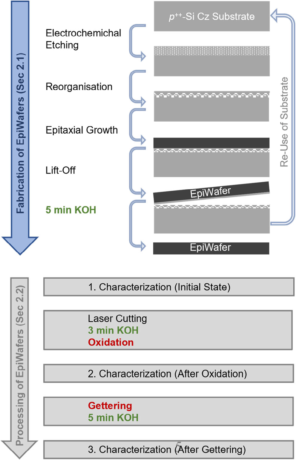
The concept of EpiWafers aims to reduce energy, cost, and material usage in wafering by growing silicon epitaxially on a reusable substrate. This process involves several steps, as illustrated in Figure 1: The highly pþ-doped Cz-Si substrate was electrochemically etched with varying currents to form a stack of porous silicon layers (PorSi) that was reorganized subsequently during a step at temperatures above 1000 °C. After reorganization, the PorSi consisted of a closed, monocrystalline surface, acting as a template during epitaxial growth, and a highly porous layer underneath, acting as a detachment layer after epitaxial growth.

Figure 1. Schematic of EpiWafer production and substrate reuse cycle (blue arrow) as well as schematic of further processing and characterization (gray arrow) in this contribution with KOH etching steps in green color and high-temperature processing steps in red color.
After reorganization, Si was grown epitaxially on the substrate with the PorSi by chemical vapor deposition (CVD) using trichlorosilane (TCS) as precursor. The epitaxially grown layers were mechanically lifted off from the substrate which could be reused for the next EpiWafer fabrication.In the following sections, we name the EpiWafer’s surface that was in contact to the substrate the EpiWafer’s backside, whereas the top of the epitaxially grown layers is referred to as the EpiWafer’s frontside.
2.2. Characterization Methods
In this contribution, we evaluated the material quality of the EpiWafer with respect to electrical as well as crystallographic properties.
The minority charge carrier lifetime, as an electrical property of the EpiWafer’s bulk material, was assessed spatially resolved and injection dependent by photoluminescence imaging (PLI) calibrated with modulated photoluminescence, using Fraunhofer ISE’s modulum setup.The measurements were performed at various illumination intensities ranging from 0.001 to 2.5 sun equivalents (sun eqs). In this analysis, we presented lifetime images detected at an illumination intensity of 0.05 Sun eqs, ensuring an excess charge carrier density comparable to maximum power point (MPP) conditions in a solar cell made from this bulk material. Average lifetimes within a certain region of an EpiWafer were calculated by the square root harmonic mean.
3. Results and Discussion
3.1. Material Quality of EpiWafer in Its Initial State
We discuss the quality of the EpiWafer in its initial state, right after the lift-off from the substrate, the removal of PorSi residuals by 5 min of KOH etching, a chemical cleaning process, and the Al2O3 surface passivation. The electrical material quality of the EpiWafer is quantitatively evaluated through injection-dependent lifetime measurements with a subsequent analysis of its effi- ciency potential. The crystallographic material quality is then discussed quantitatively and qualitatively based on BF microscope images.
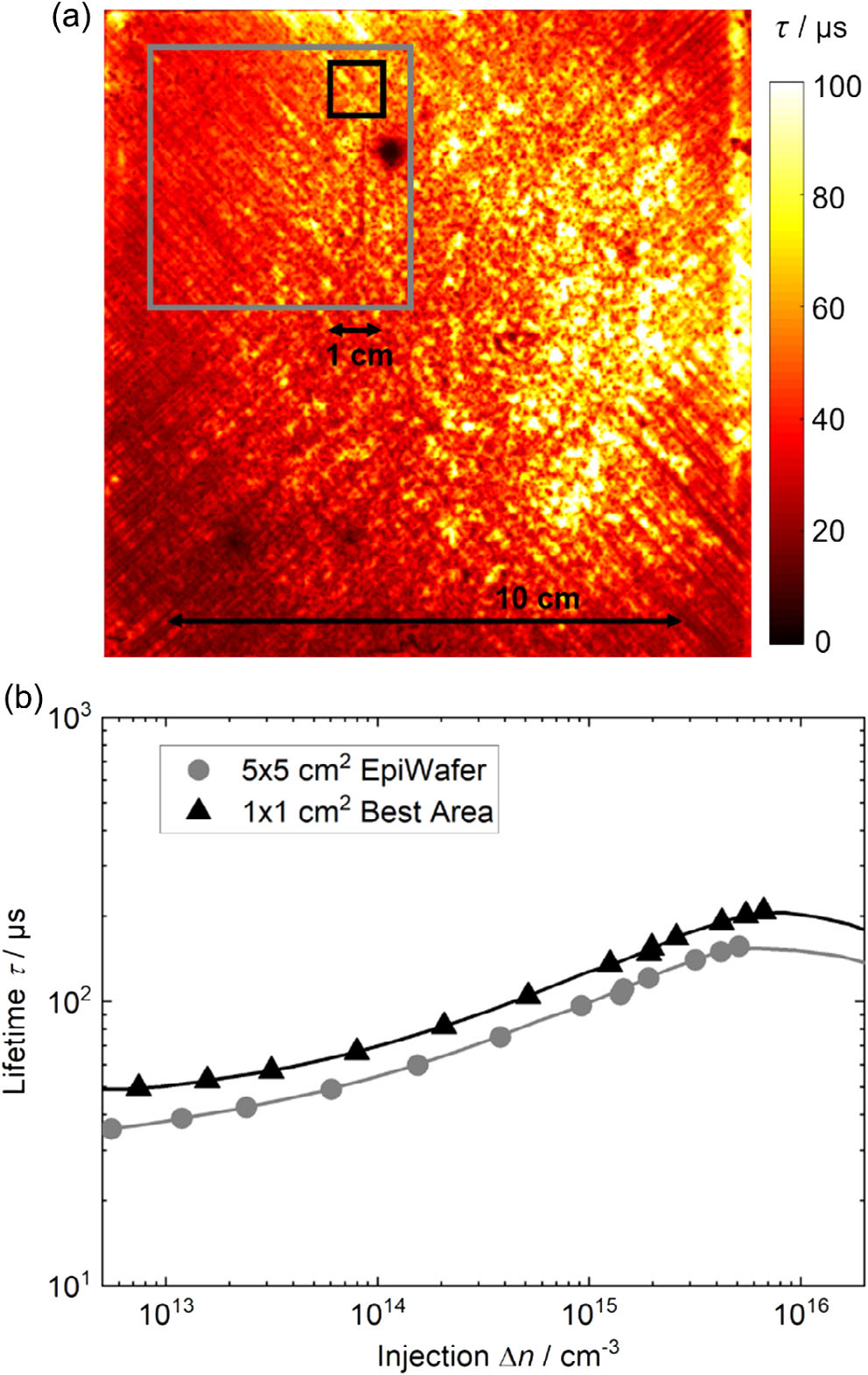
Figure 2a shows a lifetime image of the whole EpiWafer in its initial state detected at MPP conditions. The lifetime across the EpiWafer varies mainly between the corners with lower lifetimes ranging from 20 to 50 μs and the central area with higher lifetimes up to 100 μs. The average lifetime (calculated by square root harmonic mean) of the entire EpiWafer is 40 μs. Within the area of the further processed 5x5 cm2 EpiWafer after laser cutting (highlighted by the gray frame in Figure 2a), the lifetime remains essentially the same at 42 μs. The further processed 5x5 cm2 EpiWafer exhibits a more homogeneous lifetime distribution compared to the whole wafer, with the best lifetime of 58 μs within the best 1x1 cm2 area (framed in black). However, even within the further processed 5x 5 cm2 EpiWafer, there is a reduced lifetime near the corners, displaying dots of reduced lifetimes as well as lines of reduced lifetime along the <110>-direction of the EpiWafer (45° with respect to the wafer edges). This will be discussed in detail later in this article.

Figure 2. a) Lifetime image of the initial EpiWafer (125x125 mm2 ) detected at an illumination of 0.05 sun eqs by modulum at Fraunhofer ISE. The further processed EpiWafer (5x5 cm2 ) is framed in gray and the best 1x1 cm2 within this area is framed in black. b) Average injection-dependent lifetime of the gray and black framed areas with an interpolation according to ELBA.
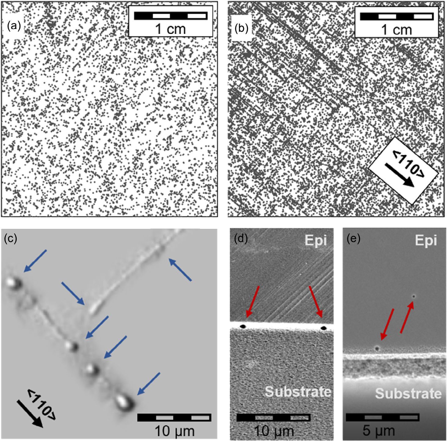
To correlate the patterns of enhanced recombination with structural crystal properties, we analyzed BF microscope images after defect selective etching. Figure 3a shows a mapping of EPs, representing penetrating dislocations, on the frontside of another, but representative EpiWafer within the central 3x3 cm2 square, while Figure 3b displays the corresponding backside. On the frontside, the EPs are randomly distributed across the EpiWafer. On the backside, however, the EPs align along the <110>-directions of the EpiWafer exhibiting a signifi- cantly higher EP density of ≈2400 cm-2 on the backside compared to 700 cm-2 on the frontside.

Figure 3. Structural defects in the EpiWafer in its initial state detected by an optical microscope. Distribution of dislocations on the EpiWafer’s a) frontside and b) backside. c) Details of the BF image of dislocations at the backside arranged along <110>-direction and connected in pairs. d) REM image of the cross section of the interfaces between epitaxially grown layers and substrate d) without PorSi and e) with PorSi. Blue arrows point at pairwise-connected EP and red arrow at MDs.
3.2. Improvement of EpiWafer’s Quality
In the previous section, we discussed the presence of structural defects at the back surface of the EpiWafer being one limitation among others like SFs and transition metals. These structural defects have a detrimental effect on the overall material quality due to carrier diffusion toward them, limiting the average minority charge carrier lifetime to a level in the range of ≈50 μs or to a predicted efficiency in the range of ≈21%.Thus, with these near-surface structural defects present, the electrical material quality of the EpiWafer is not sufficient for the fabrication of high-efficiency solar cells. In this section, however, it is shown that the material quality improves sufficiently for the fabrication of highly efficient solar cells by processing steps typical for (or compatible with) TOPCoRE solar cell fabrication, namely, KOH etching, oxidation, and gettering. We will first discuss the material improvement qualitatively by showing lifetime images after KOH etching, oxidation, and gettering. Then, detailed insights into the origin of the improvements are provided by close-up images of structural defects detected by BF microscopy and highly resolved recombination of minority charge carriers detected by μPL. Finally, the improvements are described quantitatively by discussing and comparing distinct increases in the average lifetime for each processing step and predicted efficiencies according to the TOPCoRE manufacturing route.
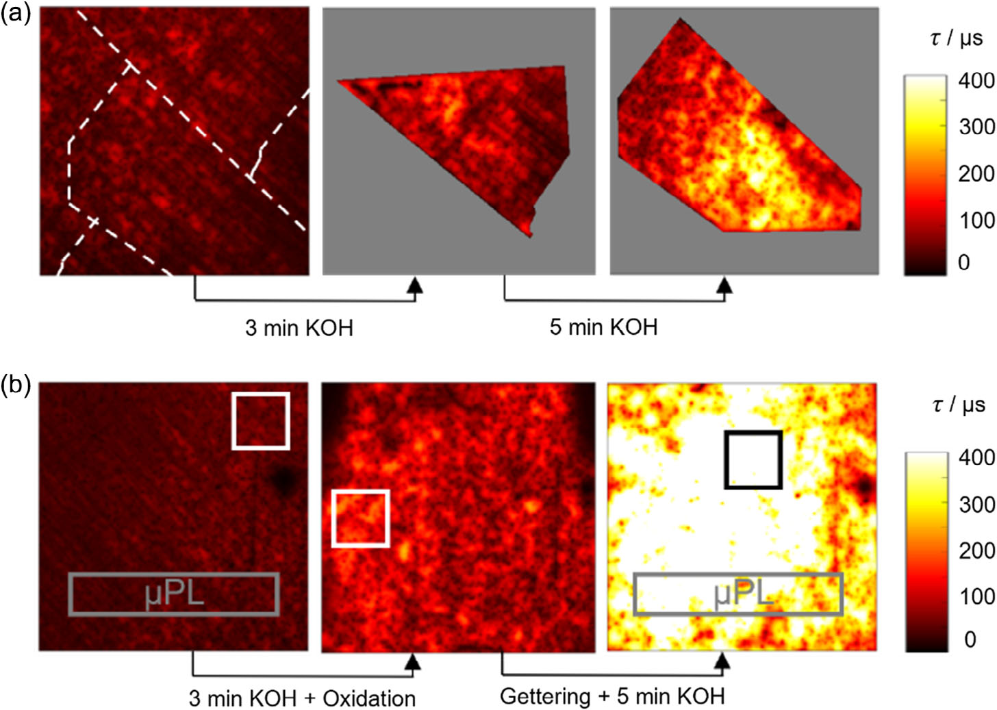
KOH etching improves the material quality by removing nearsurface structural defects at the backside of the EpiWafer. Figure 4a illustrates lifetime images of an EpiWafer in its initial state (left), a piece of the same EpiWafer after 3 min of KOH etching (middle), and another piece of the EpiWafer after 8 min of KOH etching (right). With a KOH etching rate of 1 μm per minute per side, 3 μm, respectively, 8 μm of Si were removed from both sides of the EpiWafer. Apparently, 3 min of KOH etching already enhances the overall lifetime but is not sufficient to remove all pairwise-connected MDs from the backside, as there are still many lines of reduced lifetime in <110>-direction present after etching. After 8 min of KOH etching, these lines vanish almost completely and the overall electrical quality increases drastically as the lifetime increases.

Figure 4. Lifetime images of a 5x5 cm2 EpiWafer detected at an illumination of 0.05 sun eqs by modulum at Fraunhofer ISE along the processing route of a) only KOH etching and b) high-temperature processing (oxidation and POCl3 gettering) including KOH etching steps with best 1x1 cm2 areas framed in white/black.
4. Conclusion
Demonstrating an efficiency potential above 25%, we show that p-type silicon EpiWafers, after phosphorous (POCl3) gettering at 840 °C, are suitable for the fabrication of high-efficiency solar cells. The bulk material remains stable under oxidation at 1050 °C, which is necessary for laboratory solar cell fabrication using a TOPCoRE design, and it improves significantly after gettering.
In the initial state of EpiWafers, structural defects limit the material quality and consequently the efficiency potential to ≈21%. The most detrimental structural defects are found to be dislocations at the backside of the wafer close to its surface, aligned along the <110>-direction and connected in pairs. This configuration most likely originates from MDs bending toward voids in the porous silicon layer at the substrate–EpiWafer interface. Defects close to the surface can be removed by KOH etching improving the material quality already significantly. An oxidation step has no additional effect on the EpiWafer’s quality. In contrast, the gettering has a significantly positive impact on the material quality, exceeding the effect of the accompanying etching step. This indicates that gettering most likely removes 3d transition metals from the bulk. After gettering, the main source of recombination at structural defects shifts from the nearsurface dislocations to recombination at SFs as observed through a comparison of μPL mapping and SF mapping. These SFs are highly recombination active and potentially decorated with captured transition metals that cannot be gettered, in contrast to dissolved metals.
上一篇: 用导电聚合物功能化介孔硅的晶圆级制造