ABSTRACT
Low-cost aqueous alkaline etching has been widely adopted for monocrystalline silicon surface texturing in current industrial silicon solar cells. However, conventional alkaline etching can only prepare upright pyramid structures on mono-crystalline silicon surfaces. This study demonstrates for the first time the use of ethylene glycol butyl ether (EGBE) to regulate aqueous anisotropic alkaline etching and prepare inverted pyramid structures on monocrystalline silicon surfaces. Acidic metal-catalyzed etching solutions are not the best choice for monocrystalline silicon due to their inherent disadvantages, such as noble metal pollution and relatively high costs. The one-step method to produce the inverted pyramid structures by using alkaline etch with EGBE additive is simple and inexpensive, does not generate noble metal pollution, and especially compatible with current industrial silicon solar cell production lines. With the use of a sodium hydroxide (NaOH) solution containing a low-cost additive, inverted pyramid structures can be prepared on monocrystalline silicon surface in a short time. This method is suitable for various types of silicon wafers and has great potential for industrial solar cell applications.
1. Introduction
In the past decades, silicon, which have many extremely advantageous properties such as chemical stability, high carrier mobility, and nontoxicity, have become the most important materials in the microelectronic and photovoltaic industries and are widely used in biosensors, genetic engineering, electronic devices, photonics devices, and energy technology. The technologies used to prepare the micro/nanostructures on silicon surface have always been the focus of researchers. Scientists have conducted various studies on solar cells to improve their photoelectric conversion efficiencies, and surface texturing is one of the critical technologies for improving cell efficiency. The conventional flat silicon surface has a high natural reflectivity. The average reflectivity of the flat silicon surface was around 40 %. Surface texturing refers to forming surface microstructures with different shapes on the silicon surface through various techniques to increase light absorption capability. Many texturization methods have been proposed including dry etching techniques such as plasma etching and aqueous wet techniques that involve chemical reactions in solutions. Compared to dry etching process, wet etching of crystalline silicon has been studied extensively and used widely in industry due to its low cost and suitability. Aqueous alkaline etching has been widely used in industrial production to form pyramid structures in mono-crystalline silicon solar cells. Pyramid structures can efficiently reduce the surface reflectance by extending the paths of incident photons. In the current production of monocrystalline silicon solar cells, alkaline etching has become the most widely used method for silicon surface texturization due to its low cost and environmental friendliness.
2. Experimental details
Tables 1 and 2 are all the experimental etching parameters.

Table 2 Characterization and measurement equipment.

Materials characterization
The morphologies of the samples were characterized via a high-resolution scanning electron microscope (Hitachi-SU8010). The optical reflectance measurement was performed by a UV–Vis–NIR spectrophotometer (Shimadzu, UV-3600, with an integrating sphere) in the wavelength range of 300–1100 nm. The spectral response characteristics, including IQE (internal quantum efficiency) and EQE (external quantum efficiency), were measured by a spectral response instrument (GP SOLAR, IQE-Scan). The PV cell characteristics were analyzed by hallmark.
3. Results and discussion
Generally, aqueous alkaline etching results in upright pyramids on monocrystalline silicon surface. This was discovered and has been applied since the mid-20th century. The texturization process for monocrystalline silicon wafers involves the anisotropic etching of silicon wafers in an alkaline solution containing either NaOH or potassium hydroxide (KOH). In industrial solar cell production processes, NaOH or KOH are usually chosen due to their lower costs. We were inspired to add an additive used in aqueous alkaline etching to assist in the formation of inverted pyramids. After many attempts, we successfully used an alkaline solution with added EGBE to etch inverted pyramid structures on the Si (100) surface. This is the first time that inverted pyramid structures have been prepared in one step in alkaline solutions without photolithography or secondary etching processes but through a one-step wet experimental process, as shown in Fig. 1. Fig. 1(a)–(d) are the SEM images of the inverted pyramids prepared by a one-step alkaline etching process.
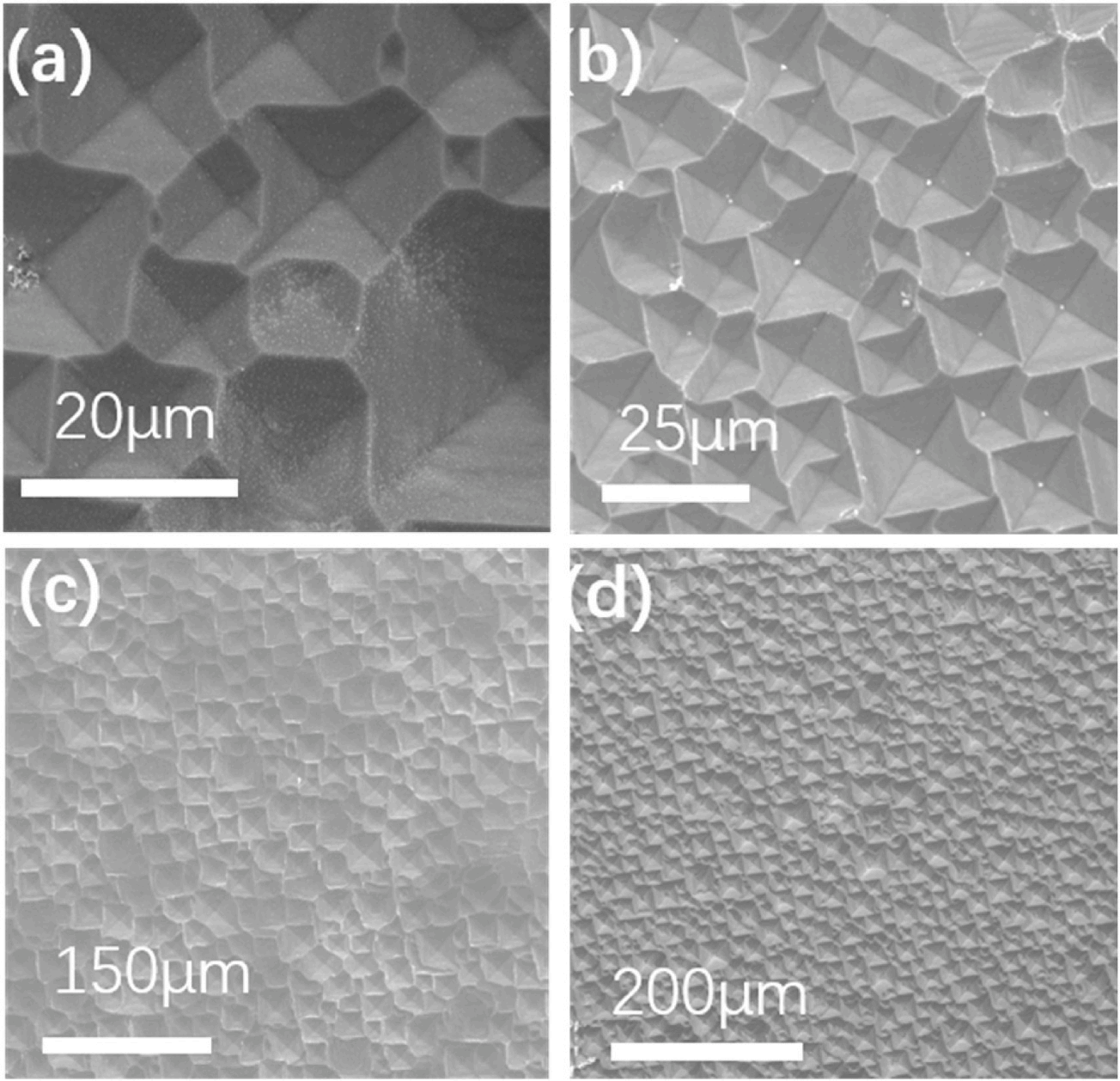
Fig. 1. Inverted pyramid SEM images with different magnifications for a p-type silicon wafer (B doped, 15–25 Ω•cm, crystal direction (100)) etched with alkaline solution.
Fig. 2 shows SEM images of the inverted pyramid cross-sections prepared by alkaline texturization. In Fig. 2, a silicon wafer with a long etching time generates large inverted pyramid structures on its surface, which clearly demonstrated the structural characteristics of the inverted pyramids. The oblique 45◦ SEM image showed that the silicon wafer surface had a very complete and regular inverted pyramid structure, and the edges of the inverted pyramids were clearly visible. The 90◦ SEM image of the cross-section also shows the downwards concave structure on the silicon wafer surface. Fig. 2(d) demonstrates that an inverted pyramid structure was made with our method.
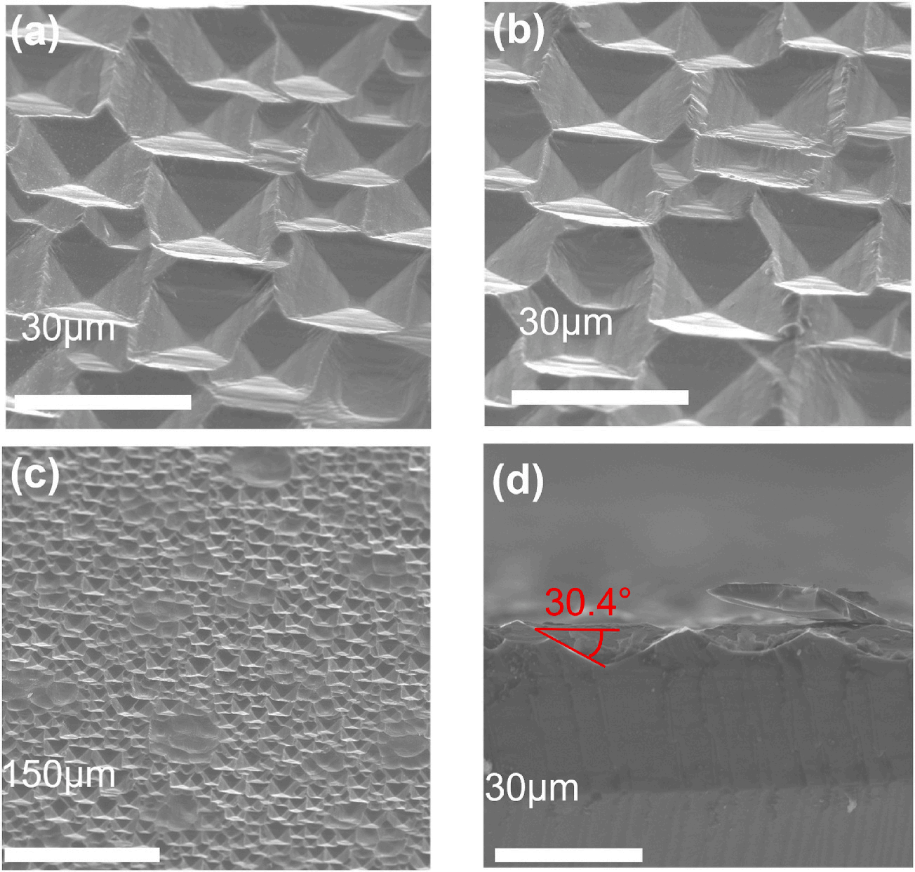
Fig. 2. SEM images with different magnifications for inverted pyramid structure sections prepared by etching p-type silicon wafers (B doped, 15–25 Ω•cm, crystal direction (100)). (a)–(c) SEM image with a 45◦ oblique view of silicon. (d) Silicon cross-sectional view shows the texture angle of the inverted pyramids. (For interpretation of the references to colour in this figure legend, the reader is referred to the Web version of this article.)
The silicon wafers with inverted pyramid structures used in the EDS analysis were not ultrasonically cleaned, and the EDS results are shown in Fig. 4. The EDS results and SEM images show that there were white substances in the pits after alkaline etching, and the pits were continually etched to form the inverted pyramid structures. The elemental analyses showed that there were several elements present, such as silicon (Si), oxygen (O), and sodium (Na). Fig. 3(a) shows the results of the EDS elemental analyses throughout the region of the image. Fig. 3(b) shows the results of the EDS scans for the elements at cross spot 1 in the image. Based on the mechanism of NaOH etching, it is inferred that the substance was sodium silicate (Na2SiO3). The silicon atoms arose because the white substance formed a thin layer, which caused the substrate silicon to be included in the EDS analysis, so silicon atoms constituted most of the silicon surface content. As shown in Fig. 3(b), due to scanning at a specific spot, Na was more prominently presented, indicating that the surface at this point contained Na, Si, and O. Therefore, we propose the following mechanism for one-step alkaline etching of silicon with EGBE to form inverted pyramid structures: since the OH− groups etched the silicon along the crystal orientation, the silicon was etched along the (100) surface, and the Na2SiO3 generated during the etching process was insoluble in the EGBE, so only the water in the solution dissolved the Na2SiO3. When the solution became saturated, the Na2SiO3 generated during the etching process was deposited on the silicon surface and acted as a mask. That is, this mechanism was basically the same as the mechanism for preparing inverted pyramid structures by photolithography masking, except that the mask used in photolithography was replaced by the Na2SiO3 produced during the alkaline etching process because Na2SiO3 is insoluble in EGBE. The mechanism is shown in Fig. 4. After Na2SiO3 formed the mask, the OH− groups continued to etch along the exposed silicon surface, and finally, Na2SiO3 was deposited at the bottoms of the inverted pyramids, as shown in Fig. 5. The addition of sodium hydroxide (NaOH) solution results in a higher etch rate and better anisotropy between the (100) and (111) crystallographic planes. The silicon atoms on Si(100) plane are etched away at a faster rate compared to those on Si(111) plane, leading to the formation of a pyramidal structure. In other wet etching solutions, such as IPA (isopropyl alcohol), TMAH water solution, oxidation agents (e.g., ferricyanide K3Fe(CN)6), anionic SDSS(sodiumdioleyl sulfosuccinate), cationic ASPEG (Acrylic polyethers), and non-ionic PEG (Polyethylene glycol)), the additives primarily serve to eliminate bubbles or accelerate the reaction process. They do not alter the results obtained with sodium hydroxide and cannot change the upright pyramids into inverted pyramids. The role of EGBE is distinct from other reported additives. Its main function is to inhibit the dissolution of sodium silicate, allowing it to accumulate on the sites where silicon has already been etched by sodium hydroxide. This protects the underlying silicon from further reaction with sodium hydroxide. As sodium silicate accumulates on these sites, combined with the different atomic structures on the (100) and (111) surfaces of silicon, it becomes more difficult for the (111) surface to be etched, resulting in the formation of an initial inverted pyramid structure. Sodium silicate then deposits downward, and when all exposed silicon crystal faces are (111), it ultimately leads to the formation of an inverted pyramid structure.
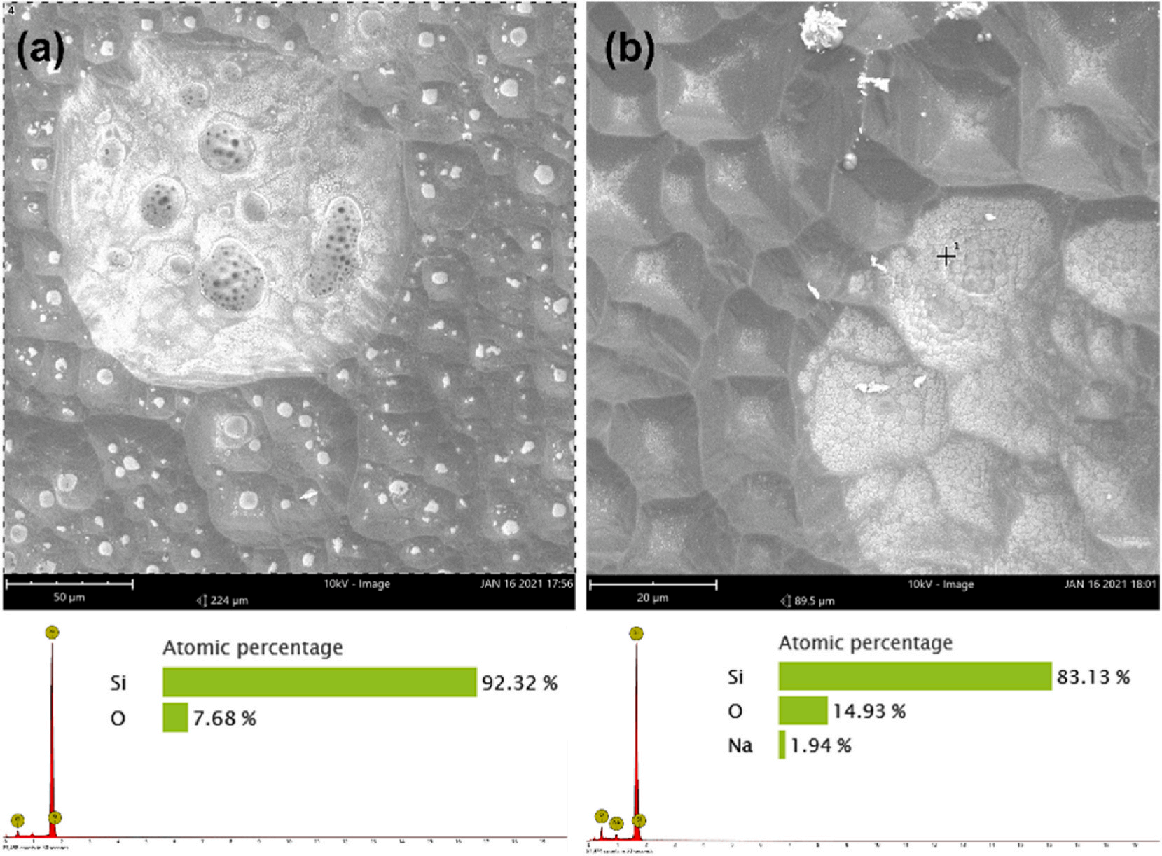
Fig. 3. Surface EDS results obtained after etching silicon wafers with an alkaline mixed solution of EGBE and NaOH. (a) EDS scans of the whole surface region in the SEM image. (b) EDS spot scanning at the cross spot. (For interpretation of the references to colour in this figure legend, the reader is referred to the Web version of this article.)
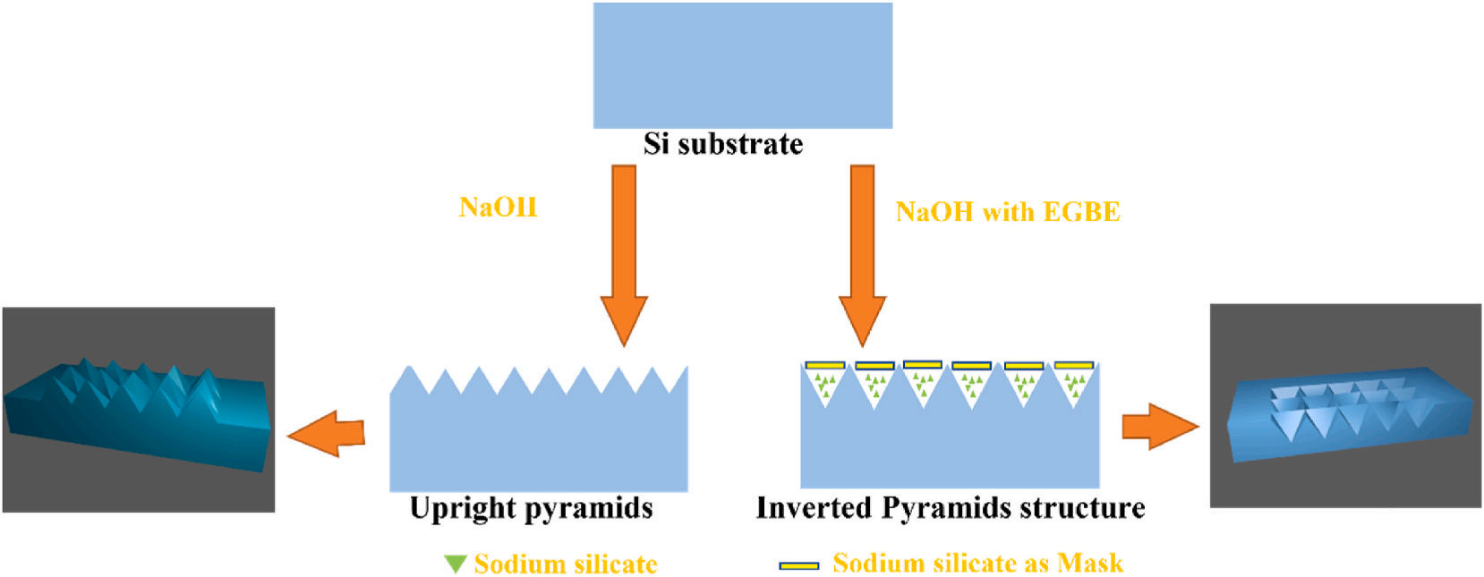
Fig. 4. Schematic diagrams of conventional alkali etching to form an upright pyramid structure (left) and the use of EGBE to regulate the etching of silicon wafers by a NaOH solution to form an inverted pyramid structure (right). (For interpretation of the references to colour in this figure legend, the reader is referred to the Web version of this article.)
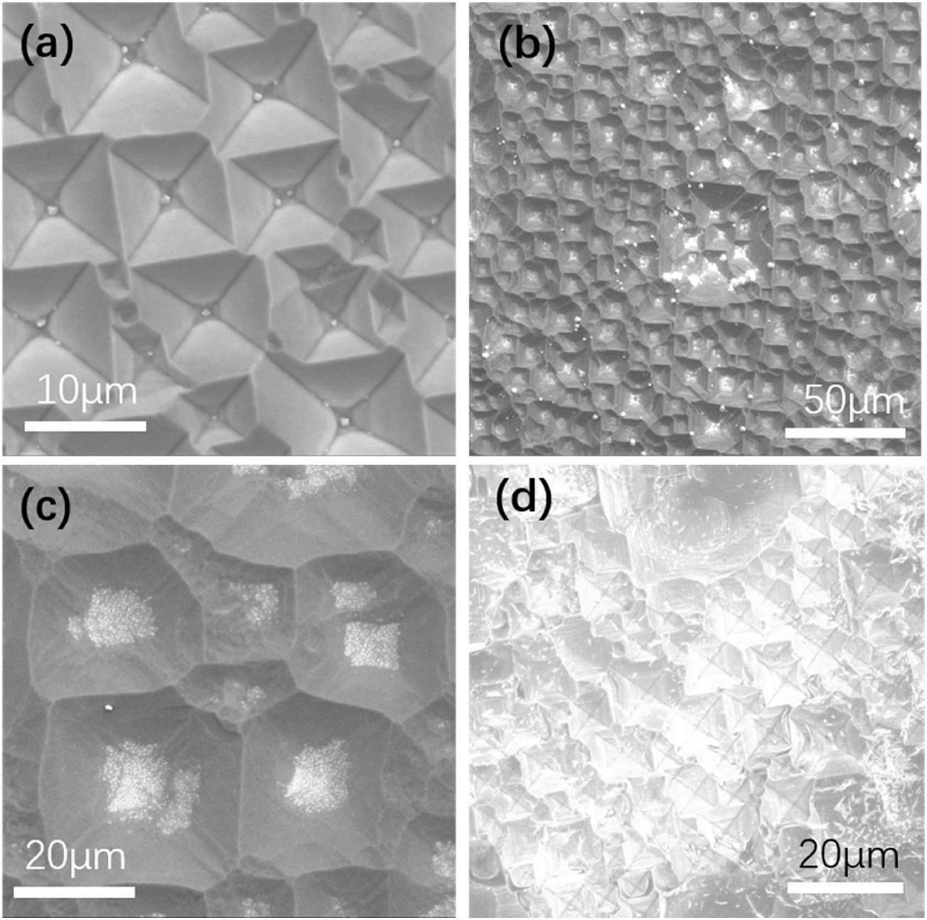
Fig. 5. SEM images of the p-type silicon wafer (B doped, 15–25 Ω • cm, (100)) formed by etching with an alkaline mixed solution of EGBE and NaOH. The silicon wafer was not ultrasonically cleaned in (d).
4. Conclusion
Inverted pyramid structures were successfully prepared on silicon surfaces with alkaline solutions. This experimental method was the first to use a one-step alkaline etching method to etch inverted pyramids on a monocrystalline silicon wafer. The inverted pyramid structures prepared by alkaline etching showed regular shapes and sizes that met the requirements for silicon solar cells. This method can be applied to different types of polished or diamond wire-cut silicon wafers. Based on many experiments, we proposed a mechanism for preparing inverted pyramid structures by alkaline etching. We believe that the added EGBE blocked the dissolution of Na2SiO3 during the alkaline etching process, which caused the Na2SiO3 to deposit on the silicon surface and act as a mask. Combined with alkaline anisotropic etching, this led to the formation of inverted pyramid structures. Additionally, this paper provides a mechanistic explanation for the preparation of inverted pyramids by alkaline etching. After etching, some white solid remained on the silicon surface, which quickly dissolved when placed in water. Based on the alkaline etching process and the EDS element analyses, it is believed that the white solid was Na2SiO3, which is the only product from alkaline etching other than water. Because Na2SiO3 became saturated in the water and is insoluble in EGBE, it precipitated on the silicon surface and acted as lithography masks, allowing hydroxide to etch the uncoated areas of the silicon surface and thus form the inverted pyramid structures, as in photolithography. The inverted pyramid structures prepared by alkaline etching exhibited a lower reflectivity than the conventional upright pyramid structure and flat polished silicon wafer. In addition, we fabricated mono-crystalline silicon solar cells with inverted pyramid structures using this method. The resulting cells exhibited an efficiency of 21.54 %, illustrating the applicability of this alkaline etchingbased inverted pyramid fabrication method in solar cell manufacturing.