Abstract: The application range of fused silica optical components can be expanded and the cost of fused silica components can be reduced by depositing the same material film on fused silica substrate. However, due to the different manufacturing process, the performance of ALD SiO2 film is lower than that of fused silica substrate, which also limits the use of this process. In this paper, ALD SiO2 film with different thicknesses were deposited, and then the structure and properties were tested. Finally, the ALD SiO2 film was treated via the annealing process. Transmission electron microscopy (TEM) showed that the ALD SiO2 film had good compactness and substrate adhesion. The Raman spectra showed that the ALD SiO2 film and substrate had the same structure, with only slight differences. The XRD pattern showed that ALD-fused silica did not crystallize before or after annealing. The infrared spectra showed that there was an obvious Si-OH defect in the ALD SiO2 film. The laser damage showed that the ALD SiO2 film had a much lower damage threshold than the fused silica substrate. The nanoindentation showed that the mechanical properties of the ALD SiO2 film were much lower than those of the fused silica substrate. After a low-temperature annealing treatment, the ALD SiO2 film Si-OH defect was reduced, the ALD SiO2 film four-member ring content was increased, the elastic modulus of the ALD SiO2 film was increased from 45.025 GPa to 68.025 GPa, the hardness was increased from 5.240 GPa to 9.528 GPa, and the ALD SiO2 film damage threshold was decreased from 5.5 J/cm2 to 1.3 J/cm2 .
1. Introduction
Current global concerns about energy resources are seeing a shift towards sustainable energy generation technologies. Inertial fusion energy (IFE) is a new type of energy that obtains clean deuterium tritium (DT) fusion energy based on inertial confinement fusion (ICF) and has commercial application value. The drive device of laser inertial confinement nuclear fusion is a large and complex optical system that requires a large number of highquality optical components. Fused silica is the amorphous state of silicon dioxide; has excellent heat resistance, with a melting point temperature as high as 1730 ◦C; can work at a high temperature of 1450 ◦C for a short time; has excellent transmittance in far ultraviolet light, visible light, and near infrared light; has higher mechanical properties than ordinary glass; and has a manufacturing process. Because of these excellent properties of fused silica, it is often used as a basic material for optical components. Taking the National Ignition Facility (NIF) built in the United States in 2009 as an example, there are 1728 fused silica windows and lenses in the diameter range of 0.5 to 1.0 m and 192 fused silica gratings and shields. The Laser Megajoule (LMJ) device in France and the Shen Guang III series device constructed in China also use a large number of fused silica components. The most common method for producing fused silica workpieces is grinding. Due to the high hardness and low fracture toughness, fused silica is removed in brittle mode in the grinding process. Crack propagation is the main way to remove fused silica. Because the median crack is deep inside the fused silica, it cannot be removed during the grinding process. This leads to the inevitable existence of micro-cracks on the surface of the fused silica component. These micro-cracks can cause the enhancement of light intensity, which in turn causes the components to produce a large number of damage points of varying sizes under the laser density below its inherent damage threshold. When the fused silica is polished, the cutting depth is very small, the cracks are also very small, and the defects are few. In order to reduce the surface defects of fused silica components, polishing and other precision processes are often used to manufacture fused silica components, which leads to long manufacturing cycles and high processing costs. Atomic layer deposition (ALD) is a coating technique based on the sequential reaction of gaseous reactants limited to the solid surface of the substrate. As a result, the ALD process can manufacture optical film with ultra-high uniformity and excellent thickness accuracy in local and large areas.
2. Experimental Process
2.1. Sample Preparation
Fused silica substrate with a surface roughness of less than 2 nm (RMS) was polished before deposition. The substrate thickness was 2 mm. The silicon wafer substrate was polished before deposition and had a surface roughness of less than 2 nm (RMS). Prior to deposition, all substrates were ultrasonically cleaned with a mixture of deionized water and ethanol. Then, the fused silica substrate was chemically etched in a 5% hydrofluoric acid solution for 80 min to remove absorbed impurities (Ce, Fe, etc.) and passivation . The substrate was then rinsed with deionized water to clean the surface. By measuring the height of the corroded part from the original surface, the corrosion depth was calculated to be about 4 µm. In beneq TFS 500, using BTBAS as a Si precursor and O3 as an oxygen source, a single SiO2 film was deposited on the previously prepared fused silica substrate and silica wafer substrates via the thermal ALD method at substrate temperatures of 300 ◦C. Per the typical ALD cycle, the first step was filling it with BTBAS for 0.5 s, the second step was filling it with nitrogen for 3 s, the third step was filling it with O3 for 2s, and the last step was filling it with nitrogen for 3 s. The film thickness and growth rate of the deposited SiO2 were measured via spectroscopic ellipsometry. In our experiment, the growth rate of ALD SiO2 was 0.1 nm/cycle. In a super-clean room, samples were placed in Petri dishes and wrapped in tinfoil and then annealed in a box-type resistance furnace (Model: KXL-1200X, Hefei, China). The samples were heated at rate of 10 ◦C/min, then held for 1 h, and last, cooled to normal temperature in the furnace.
3.Experimental Results and Analysis
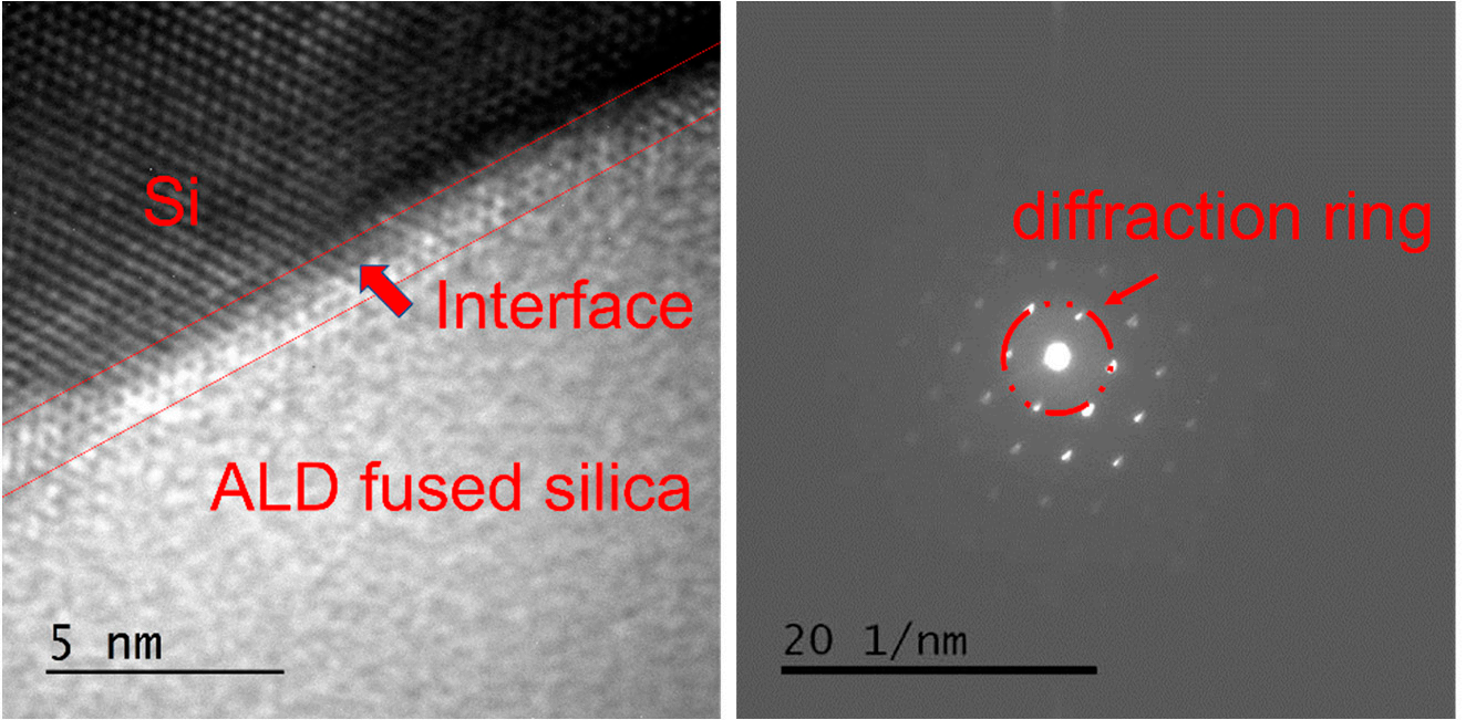
lransmission electron microscopy can be used to observe the crystal structureof a sample and is commonly used to study the structure of thin film. ALD SiOfilm on silicon wafer substrate was studied via transmission electron microscopy, and theimages obtained are show in Figure 1. Periodic arrangement of atoms in crystals can yieldregular dark field images. It can be seen in Figure la that the ALD SiO, film had a clearinterface with the substrate, and the interface width was about 1.5 nm, which was closeto the roughness of the silicon wafer. There were no obvious micro-defects such as holesor cracks at the interface, indicating that the adhesion of the atomic layer deposition wasexcellent. The accelerated and concentrated electron beam was projected onto a very thinsample, and the electrons collided with the atoms in the sample and changed directionthus obtaining an image of the atomic positions and defects. The upper left corner depictsobvious crystal silicon lattice characteristics, whereas the lower right corner shows that theALD SiO, had no crystal lattice characteristics. After electrons passed through the sampleelectrns from the same direction were focused on the same point behind the objective lensresulting in an electron diffraction pattern. Because the atoms of a crystal have periodiclaws, in a crystal material, the diffraction image is composed of a series of regular lightspots. Because the atoms of amorphous materials lack the periodic rule of long-range orderthe diffraction image turns out to be dispersed concentric circles. The electron diffractionpattern at the interface was obtained via diffraction operation on the ALD SiO,, as shownin Figure lb. Because the electron beam diameter was much larger than the interface widththe diffraction ring fommed by the ALD SiO, and the reciprocal lattice formed by the crystal.

Figure 1. Transmission electron microscopy (TEM) photo of ALD SiO2 on silicon wafer substrate. (a) Lattice image of film interface and (b) electron diffraction pattern at the interface.
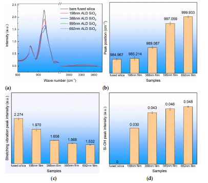
The atoms that make up chemical bonds or functional groups are in a state of constant vibration, and their vibration frequency is comparable to that of infrared light. When organic molecules are irradiated with infrared light, the chemical bonds or functional groups in the molecules can be vibrationally absorbed, and different chemical bonds or functional groups have different absorption frequencies, specifically in different absorption peak positions in the infrared spectrum. In this way, the structure of the samples could be obtained by detecting the position of the infrared absorption peak. Infraredspectrum tests were carried out on different thicknesses of ALD SiO, film on fused silicasubstrate, and the results are shown in Figure 2. Each sample was measured at threedifferent locations. The structure of the ALD SiO, film was the same as that of the fusedsilica substrate, both of which contained a stretching vibration mode and a stretchingvibration mode of Si-0. In Figure 2a, the measurement of 980 cm-1 is attributed to Si-asymmetric stretching vibration (Vs),784 cm1 to Si-0 bending vibration (Vb), and950 cm and 3300 cm to Si-OH vibration. It can be seen in Figure 2b that theasymmetric stretching vibration peak position was related to the film thickness and thatthe vibration peak position gradually increased with the in crease in film thickness. It canbe seen in Figure 2c that the asymmetric stretching vibration peak intensity was related tothe film thickness and that the peak intensity decreased with the increase in film thicknessIt can be seen in Figure 2d that the peak intensity of Si-OH increased with the increase infilm thickness. It can be judged that the structure of the ALD SiO, film was almost thesame as that of the fused silica substrate. The ALD SiO, film contained Si-OH defect andthe peak strength of the asymmetric tensile vibration was weaker than that of the fusedsilica substrate.

Figure 2. Infrared absorption spectra of ALD SiO2 film and fused silica substrate and related vibration peak position and peak intensity. (a) Infrared absorption spectra, (b) asymmetric stretching vibration peak position of Si-O-Si, (c) asymmetric stretching vibration peak intensity of Si-O-Si, and (d) Si-OH peak intensity.
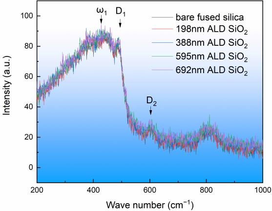
Raman spectroscopy is an analytical method based on the Raman scattering effect discovered by Indian scientist C.V. Raman. It analyzes the scattering spectra with different frequencies of incident light to obtain information about the molecular vibration and rotation, and it is applied to the study of molecular structure . It is generally believed that fused silica is a spatial network topology composed of a silicon atom and an oxygenatom tetrahedron as the basic unit. In the middle range, silicon and oxygen atoms areconnected to each other to form ring structures, such as three-membered rings, four.membered rings, and higher-membered rings. In this experiment, fused silica substrateand ALDSiO, film with different thickness were tested by Raman spectrum, and the testresults are shown in Figure 3. Each sample was measured at five different locations, In theRaman spectrum, 440 cm-1 (w,) is attributed to oxygen atoms in the ring structure withmore than five silicon atom rings, 490 cm1 (D,) is attributed to the vibration of oxygenatoms in the four-membered ring, 606 cm-1 (D,) is attributed to the vibration of oxygenatoms in the three membered ring, and 800 cm is attributed to the bending vibration ofSi-0-Si . It can be seen in Figure 3 that the peak shape and the peak position of theALD SiO, film were consistent with those of the fused silica substrate, indicating that theALD SiO, film and the fused silica substrate had the same structure.

Figure 3. Raman spectra of ALD SiO2 film and fused silica substrate.
5. Conclusions
By using BTBAS as an Si precursor and O3 as an oxygen precursor, a single layer of ALD SiO2 film was deposited on the silicon wafer and on the fused silica substrate, respectively. High-resolution electron microscopy was used to study the ALD SiO2 crosssection. The results show that the deposited SiO2 had good densification, there were no cavities or other microscopic defects in the internal or interface of the film, and the ALD SiO2 coincided with a typical amorphous state. The XRD spectra show that the ALD SiO2 did not crystallize after low-temperature annealing. The Raman spectra show that the structure of the ALD SiO2 was consistent with that of the fused silica substrate. The infrared spectrum detection shows that the ALD SiO2 asymmetric stretching vibration peak position was greater than that of the fused silica substrate, the ALD SiO2 asymmetric stretching vibration peak intensity was smaller than that of the fused silica substrate, and at the same time, the ALD SiO2 Si-OH peak was greater than that of the fused silica substrate and was proportional to the film thickness. The damage test of the ALD SiO2 film on the fused silica substrate shows that the laser damage threshold decreased with the increase in film thickness. The nanoindentation test shows that the hardness and the elastic modulus of the ALD SiO2 were much lower than those of the fused silica substrate. After annealing at a low temperature with a rapid warming rate, the ALD SiO2 four-member ring content increased, the peak position of the asymmetric stretching vibration of Si-O-Si decreased, the peak Intensity of the asymmetric stretching vibration of Si-O-Si increased, the peak intensity of Si-OH decreased, the laser damage threshold of the ALD SiO2 was reduced, the elastic modulus of the ALD SiO2 increased from 45.025 GPa to 68.025 GPa, and the hardness increased from 5.240 GPa to 9.528 GPa.