ABSTRACT
In this work, the characteristics of the gallium oxide (Ga2O3)/diamond heterostructure were thoroughly examined after the preparation of Ga2O3 thin film on bulk diamond via atomic layer deposition. The X-ray diffraction (XRD) analysis revealed the Ga2O3 film amorphous and diamond polycrystalline. The atomic force microscopy (AFM) mapping displayed remarkably smooth surfaces of the Ga2O3 film and diamond substrate (RMS of 0.184 and 0.508 nm, respectively). The scanning electron microscopy (SEM) images showed conspicuous grains formed on the diamond, and small crystallites on the surface of the film. The optical characteristics were investigated via spectroscopic ellipsometry (SE) and UV/Vis/NIR spectrophotometer. Raman spectroscopy suggested a sharp diamond-related (sp3 ) peak and an extremely weak bulge band around 1350–1620 cm−1 . X-ray photoelectron spectroscopy (XPS) analysis indicated Ga2O3/diamond heterojunction to be staggered (type II) band alignment with valence band and conduction band offsets of around 1.18 eV and 2.09 eV, respectively. Moreover, according to time-domain thermoreflectance (TDTR) measurements, the thermal conductivity of Ga2O3 and the thermal boundary conductivity of the heterointerface were 5.13 W/(m⋅K) and 19.22 MW/(m2 ⋅K), respectively. These findings not only demonstrate the feasibility of Ga2O3-on-diamond hetero-integration but open up new prospects for the design and physical analysis of Ga2O3/diamond-based devices in the future.
1. Introduction
In recent years, gallium oxide (Ga2O3) as a representative of ultrawide bandgap semiconductors has become a viable candidate for the next generation of semiconductor materials. Its bandgap (4.5–4.9 eV) wider than those of SiC (3.2 eV) and GaN (3.39 eV) causes the outstanding critical electric field of ~8 MV/cm and Baliga’s figure of merit (BFOM) of 2870, which is very attractive for the applications in ultra-high voltage electronics . It is reported that Ga2O3 crystals grown by the liquid phase melt method have dislocations less than 102 cm−2 , which is two orders of magnitude lower than that in SiC grown via gas phase technology . The improved quality of Ga2O3 single crystals greatly inspires the advancement of Ga2O3-based power electric devices. Wenshen L. et al. successfully achieved a maximum breakdown voltage (BV) of 2.89 kV in Ga2O3 trench Schottky barrier diodes (SBDs) by employing a field plate design. Using a similar design approach, Shivam S. et al. have realized an exciting breakthrough in Ga2O3 MOSFET, reporting an ever-recorded maximum breakdown voltage of 8.03 kV therein.
2. Experimental procedure
2.1. Preparation of the Ga2O3 film on the diamond substrate
Ga2O3 films were grown on the ~300 μm thick single-face polished poly-crystalline diamond bulk substrates using an ALD facility equipped with a TFS200 reactor. Before the Ga2O3 film deposition, the diamond wafers were subjected to a sequence of pretreatments, which included RCA cleaning, rinsing with deionized water, and drying under a N2 flow. The pretreated diamond wafers were then transferred into the Ga2O3 growth reactor for subsequent deposition of ~80 nm thick Ga2O3 films. Trimethylgallium (TMGa) and high-purity O2 (99.995%) were selected as the Ga and O precursors in the alternating cycles, respectively. Ar served as both the carrier and purge gas during the Ga2O3 preparation. For safety reasons, the container for TMGa was made of stainless steel, and the storage temperature was 10 ℃. The deposition conditions were kept stable (the growth temperature of 200 ℃, the pressure of ~1 mbar, and the O2 plasma activation power of 200 W). After the completion of all preparatory works, Ga2O3 films were deposited during predefined ALD cycles at the following parameters: the TMGa pulse of 50 ms, the Ar purging of 2 s, the plasma treatment for 10 s, and the Ar purging of 2 s. Finally, the samples were stored in the glovebox filled with N2 and taken out for short-term testing only.

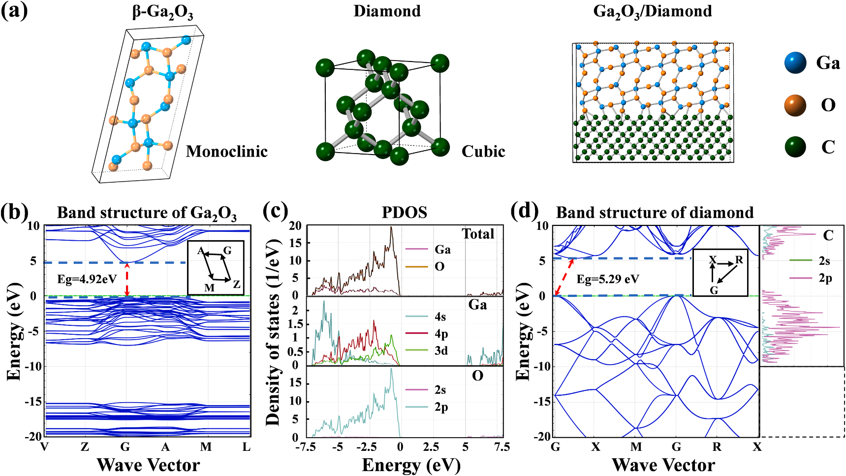
Fig. 1. (a) Schematic diagram of the crystal structure of monoclinic β-Ga2O3, cubic diamond, and Ga2O3/diamond heterostructure. (b) Band structure and (c) density of states of monoclinic β-Ga2O3. (d) Band structure of diamond.
3. Results and discussion
3.1. Analysis of band structures and densities of states of Ga2O3 and diamond
To better understand the hetero-integration of Ga2O3 and diamond, the crystal structures of monoclinic β-Ga2O3 and cubic diamond were constructed and formed Ga2O3/diamond heterostructure as shown in Fig. 1(a). Then DFT calculations were carried out to obtain the band structures and densities of states of Ga2O3 and diamond. Fig. 1(b) and (c) show the energy band structure and partial density of states (PDOS) diagrams of β-Ga2O3 with a perfect lattice, respectively. A zero energy level was referred to the Fermi surface.
3.2. Crystallinity, microstructure, and morphology
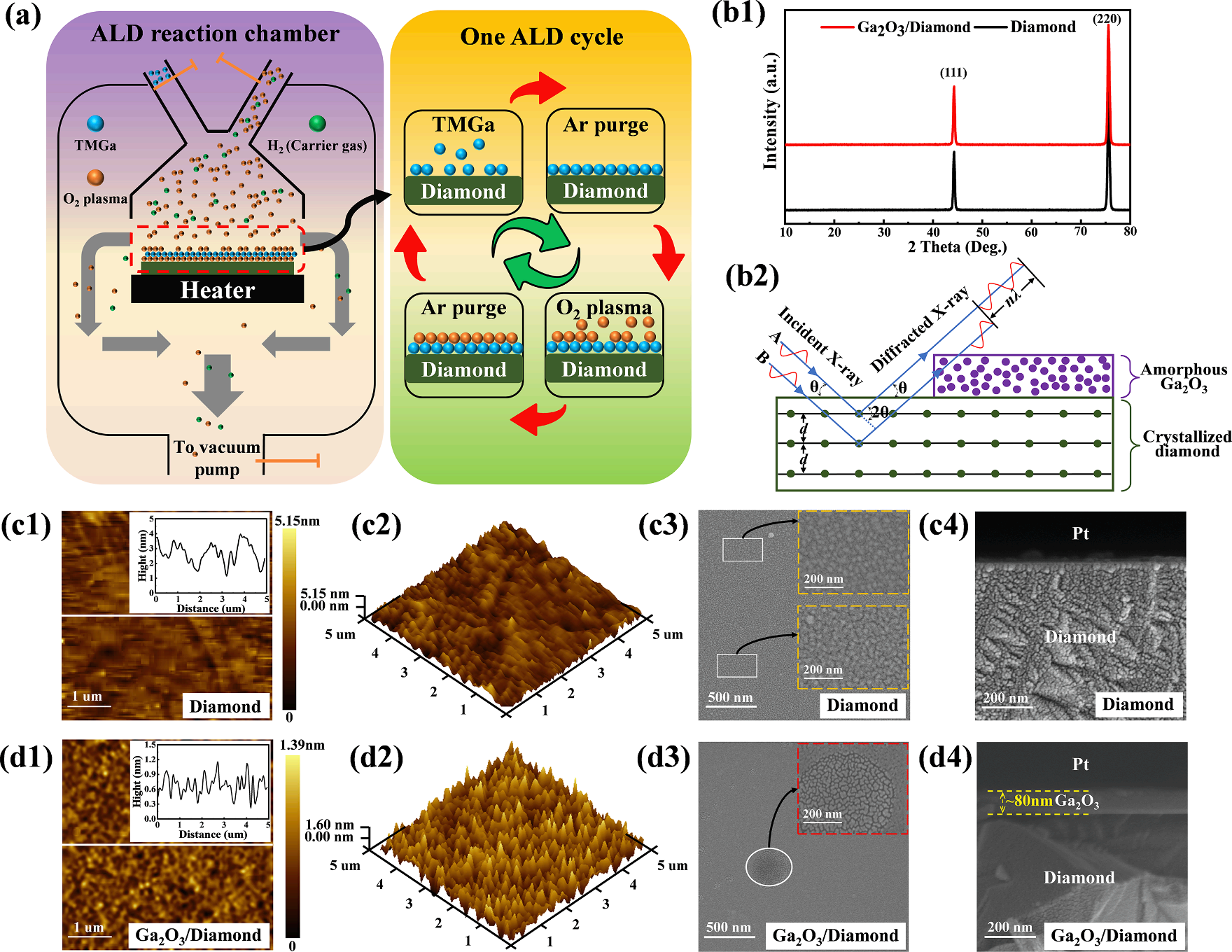
Fig. 2(a) shows typical ALD equipment and a single-cycle growth process, where the target product Ga2O3 is generated by alternately introducing the source gas reaction. To examine the crystal structure of Ga2O3-coated and pure diamond substrates, high-resolution XRD measurements were carried out in a scanning range from 10◦ to 80◦. Fig. 2 (b1) reveals two sharp diffraction peaks at 44.3◦ and 75.58◦, assigned to the (111) and (220) planes of the polycrystalline diamond substrate, respectively . Additionally, there were no specific peaks of Ga2O3, meaning that the film had an amorphous structure. According to various reports, the crystallinity of ALD-deposited films usually strongly depends on the growth temperature. For example, Richard O. et al. obtained the amorphous Ga2O3 films at relatively low temperatures (60–160 ℃). Dong-won C. et al. also claimed the films were still uncrystallized even at 250 ℃, whereas polycrystalline Ga2O3 films on the diamond were produced at 295 ℃ by Cheng Z. et al. . In this work, the temperature of 200℃ was insufficient for the surface atoms to migrate and condense into nuclei, resulting in amorphous Ga2O3. Fig. 2 (b2) depicts the schematic diagram of the XRD analysis of a Ga2O3/ diamond heterostructure, where θ, 2θ, d, λ, and n are Bragger angle, diffraction angle, interplanar crystal spacing, wavelength of X-ray, and order of diffraction, respectively. Because of the lack of crystallization, the structure of Ga2O3 was isotropic with disorderly arranged atoms therein, leading to the absence of distinct Ga2O3-related peaks in the corresponding XRD spectrogram in Fig. 2(a). Adversely, the crystalline diamond with the atomic arrangement satisfying the Bragg diffraction conditions (2dsinθ = nλ) manifested itself by strong diffraction peaks at specific diffraction angles (2θ).

Fig. 2. (a) A schematic illustration of ALD equipment and process. (b1) XRD patterns of the pure diamond, and the Ga2O3 film grown on the diamond; (b2) the corresponding schematic diagram of the structural characterization via XRD. 2D and 3D AFM images and roughness images within the area of 5 × 5 um2 of (c1-c2) the bulk diamond and (d1-d2) Ga2O3 films grown on the diamond; the insets display the height profiles along the white lines in images (c1) and (d1), respectively. (c3) Surface high-resolution SEM micrographs of the bulk diamond and (d3) Ga2O3/diamond heterostructure; cross-sectional high-resolution SEM micrographs of the diamond bulk (c4) and (d4) Ga2O3/diamond heterostructure with Pt protective layer. Insets in images (c3) and (d3) are the magnified patterns within the white rectangle and circle areas, respectively.
4. Conclusions
In this report, the Ga2O3/diamond heterojunction was prepared by ALD. Prior to the experimental part, the band structures and densities of states of Ga2O3 and diamond were described via DFT calculations. For Ga2O3, the top of the valance band and the bottom of the conduction band were mainly due to the O 2p and Ga 4s orbitals, respectively. As for the diamond, the C 2p orbital made the major contribution to the top of the valance band and the bottom of the conduction band. Subsequently, the physical, chemical, and optical characteristics were investigated systematically. It was found that the amorphous Ga2O3 thin film presented quite a smooth surface with a roughness of 0.184 nm and a welldefined coherent interface with the diamond substrate. The optical properties assessed from the SE analysis also indirectly indicated the compactness of the Ga2O3 film grown via ALD. According to the XPS measurements, the large amount of non-diamond chemical components was concentrated at the vicinity of the heterointerface compared to the surface of the uncoated bulk diamond material, which implied the partial transformation from diamond to a non-diamond phase during the preparation. At the same time, the band configuration of the Ga2O3/ diamond heterostructure was determined as staggered (type II), with the VBO and CBO values of 1.18 eV and 1.89 eV, respectively. In addition, the thermal conductivity of the ALD-prepared Ga2O3 thin film was determined to be 5.13 W/(m.K), and the thermal boundary conductivity was 19.22 MW/(m2.K). These findings provide a primary understanding of Ga2O3/diamond heterojunctions and their implementation, opening up a way to alleviate the heat dissipation problem of Ga2O3-relevant devices applied in high-power electronics and other fields. However, the large lattice mismatch and thermal mismatch between diamond and Ga2O3 are the causes of the poor interface thermal conductivity characteristics, which nullifies benefits of the initially high thermal conductivity of the diamond. In the forthcoming research, structural optimization will be taken into consideration to mitigate the mismatchrelated issues so as to enhance the interfacial thermal transport of heterojunction.
上一篇: 石墨烯的性质、合成和应用:综述
下一篇: 用于高频有机薄膜晶体管的高分辨率光刻