Abstract The chemical and physical properties of platinum (Pt) make it a useful material for microelectromechanical systems and microfluidic applications such as lab-on-a-chip devices. Platinum thin-films are frequently employed in applications where electrodes with high chemical stability, low electrical resistance or a high melting point are needed. Due to its chemical inertness it is however also one of the most difficult metals to pattern. The gold standard for patterning is chlorine RIE etching, a capital-intensive process not available in all labs. Here we present simple fabrication protocols for wet etching Pt thin-films in hot Aqua Regia based on sputtered Ti/Pt/Cr and Cr/Pt/Cr metal multilayers. Chromium (Cr) or titanium (Ti) is used as an adhesion layer for the Pt. Cr is used as a hard masking layer during the Pt etch as it can be easily and accurately patterned with photoresist and withstands the Aqua Regia. The Cr pattern is transferred into the Pt and the Cr mask later removed. Only standard chemicals and cleanroom equipment/tools are required. Prior to the Aqua Regia etch any surface passivation on the Pt is needs to be removed. This is usually achieved by a quick dip in dilute hydrofluoric acid (HF). HF is usually also used for wet-etching the Ti adhesion layer. We avoid the use of HF for both steps by replacing the HF-dip with an argon (Ar) plasma treatment and etching the Ti layer with a hydrogen peroxide (H2O2) based etchant.
1. Introduction
Platinum has a number of material properties that can be exploited in microdevices. The range of applications is diverse and there are many in which other materials simply cannot be used. It is biocompatible, inert and has a high electrical conductivity, making it an excellent choice for electrodes. Pt has a high melting point (2045 K) and its electrical resistance changes linearly over a wide temperature range, enabling its use in resistive heaters, thermocouples and resistive temperature detectors. Due to its relative mechanical hardness, it is also used as a structural material in metal flexures and switch contacts.
However, the equipment needed for reactive ion etching (RIE) of Pt is not readily available in many labs. For this reason, a number of other methods have been reported in the literature: these include additive techniques such as lift-off and shadow masking, and subtractive patterning by wet etching. The limiting factors compared to dry etching are the feature sizes and aspect ratios that can be obtained.
2. Fabrication
Multilayers with either Ti or Cr as permanent adhesion layer, a functional Pt layer, and Cr as a temporary masking layer were sputtered onto various 4" wafer substrates such as borofloat glass (PlanOptik, Germany), Si with native oxide and Si with 200 nm SiO2 (SiMat, Germany).
2.2. Sputter deposition
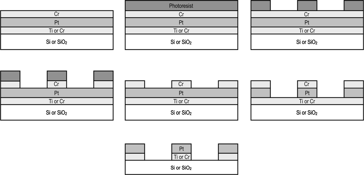
Immediately following sputter cleaning Cr/Pt/Cr multilayers were deposited in the same Nordiko RFG 2500 parallelplate RF sputter coater without breaking the vacuum (see figure 1(a)). A 72 nm Cr adhesion layer, followed by a 410 nm Pt layer and a 72 nm thick Cr masking layer was deposited.

Figure 1. Process flow for the wet etching of platinum features using a chromium hard mask: (a) multilayer metal deposition; (b)–(d) photolithographic patterning of chrome hard mask; (e) removal of photoresist and platinum surface activation; (f) Pt etch in Aqua Regia; (g) removal of exposed adhesion layer and Cr hardmask.
4" wafers were cleaned in an O2/Ar plasma in an Oxford Instruments Plasmalab 80 RIE and primed with hexamethyldisilizane (HMDS, Chestech, UK). An 800 nm thick layer of Shipley S-1813 (Chestech, UK) resist was spun onto the wafer (see figure 1(b)) and softbaked. The wafer was exposed in a maskaligner to a chrome mask and then developed in undiluted Microposit MF-319 (Chestech, UK). Resist residue in the developed areas was removed in the PlasmaLab RIE with a short O2 plasma descum step before hardbaking the resist (see figure 1(c)). The Cr top layer was wet etched by immersing the dry wafer in freshly prepared CR- 14 equivalent etchant (22% ceric ammonium nitrate, 9% acetic acid and 69% DI water, by weight) (see figure 1(d)). The Cr underetch was checked with an optical microscope and the wafer soaked overnight in acetone to strip the resist mask. Any remaining resist was cleaned off in an O2 plasma. It is essential to remove the Pt surface passivation caused by the O2 plasma resist strip. This was achieved by exposing the wafer/Pt surface to a pure Ar-plasma immediately prior to starting the Pt etch (see figure 1(e)).
3. Results and discussion
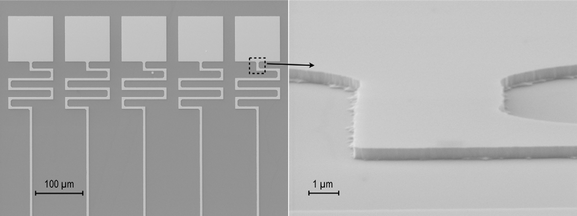
Pt layers usually require a thin adhesion layer of e.g. Cr, Ti, Ta, Ti/W. For Cr/Pt/Cr films both Cr layers should be chosen to be of the same thickness to minimize any underetch of the Cr adhesion layer during the removal of the Cr masking layer. Choosing the same Cr thickness has the additional advantage of making it easier to detect when the top Cr masking layer has been removed. This is especially easy if the substrate is a glass wafer as the contrast between a thin Cr layer and a pure glass wafer is easily detectable. A Cr adhesion layer can also withstand a KOH etch, should this be required in a subsequent deep silicon etch. Replacing the Cr adhesion layer with a Ti adhesion layer has other advantages. Ti is a better choice for high temperature applications (up to 600 ℃). Ti acts as a diffusion barrier and prevents interdiffusion to e.g. a silicon substrate and vice versa. The Ti adhesion layer is not attacked during the final removal of the top Cr masking layer and its thickness can therefore be chosen independent of the Cr thickness. In this case the Ti should be chosen with a typical adhesion layer thickness of around 30 nm. This again results in lower underetch of the Ti, which in turn allows the etching of finer Pt features. Figure 2 shows a typical etch result from a Ti/Pt/Cr sandwich structure, with clean, well defined structures. The EDX maps match the SEM and confirm that the Cr hard mask has been completely removed, revealing the Pt surface. The Pt structures have an excellent surface quality, with no pits or pinholes (see figure 3).

Figure 2. (a) SEM image and (b) corresponding EDX spectrum showing complete removal of the Cr mask from the Pt electrodes. The peak labelled EP is the detector escape peak.
The square pads on figure 3(a) had an edge length of 100 μm on the original masks. The Pt structures have an edge length of 98 μm, indicating a 1 μm underetch on either side. The inset, figure 3(b)) shows an enlarged area of figure 3(a) at an 80 degree tilt angle. The width of the meandering Pt trace is 5 μm, down from 10 μm on the original etch mask, indicating a 2.5 μm underetch on either side.
The smaller underetch of the larger structures compared to the smaller ones (see figure 3) may be due to depletion of etchant where more Pt is available for etching. This may also explain the differential etching seen on inside and outside edges of the meandering Pt trace, more easily seen in figure 2(a).

Figure 3. SEM images of wet etched Pt on a Ti adhesion layer.
4. Conclusions
A simplified method for Pt wet etching that does not require access to any equipment beyond that available in a basic MEMS lab is presented. The technique requires the deposition of only one additional Cr layer, which is patterned photolithographically and serves as a hard mask for the Aqua Regia Pt etch.