ABSTRACT
In this paper the first part of complete technological process of manufacturing crystalline silicon solar cells using screen-printed technology realised in the Photovoltaic Laboratory of Institute of Metallurgy and Materials Sciences of the Polish Academy of Sciences is presented. The setting-up of diagnostic-measurement stations in PL IMMS PAS, which are being utilized to making material parameters characteristic and which are being employed in the technology of solar cells manufacturing are described. The investigation in Photovoltaic Laboratory of IMIM of PAS are focused on crystalline solar cells. For this reason the main parameters of silicon plates using as a base material in solar cells technology are presented. Summarising, this paper gives also o brief overview on the research activities of the Photovoltaic Laboratory of PAS and their research and development equipment.
INTRODUCTION
At present the photovoltaics is one of the fastest-growing technologies in the world and photovoltaic (PV) industry shows remarkable progress. Today, nearly 90% of the worldwide solar cell production was dominated by the use of crystalline silicon (monocrystalline, multicrystalline and ribbon). The dominance of crystalline Si in photovoltaics can probably be ascribed partly to the knowledge about Si, which has accumulated in recent years in microelectronics technology. Besides, measured by mass, silicon makes up 25.7% of the Earth's crust and is the second most abundant element in the crust, after oxygen. We can say it is unlimited source of base material for solar cells. Moreover, silicon solar cell based on crystalline silicon reach high efficiency whereas their costs production are decreasing.
The cause behind constant production increase and the progress in research on photovoltaic cells technology is the customers requirement. In the year 2008 the total world power of photovoltaic systems amounted to 14 730 MW. It is also worth emphasizing that the scale of single undertakings in the field of solar energy acquisition by photovoltaic cells is constantly increasing. We can take as an example The Lieberose Solar Power Plant in Eastern Germany, which is the second biggest power plant in the world. This power plant will be producing up to 53 MW finally. It will be enough to provide electrical energy up to 50 000 of habitants. The cost of investment amounted to 160 millions of euro.
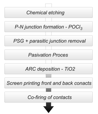
The Photovoltaic Laboratory of Institute of Metallurgy and Material Sciences of The Polish Academy of Sciences (PL IMMS PAS) in Cracow has developed the manufacturing technology of solar cells based on crystalline silicon. This technology is being realized at the experimental line in The Photovoltaic Laboratory of The Institute of Metallurgy and Material Sciences of PAS at Kozy. [1] Individual technological steps in the form of the chart shows the figure number 1.

Fig. 1. The flow chart mono and multicrystalline solar cells processing at IMIM PASs.
The research activity of the team of photovoltaic laboratory is focused on mono- and multicrystalline silicon thick films solar cells technology. There are elaborated and curried out all processes allow for complete make the silicon solar cells. Average efficiencies 16 % on textured monocrystalline silicon and above 13 % on multicrystalline silcon have been achieved. This cell efficiency has been obtained in a simple cell processing sequence.
Current research activity is focused on subjects:
1.chemical etching, texturization and cleaning for Si wafers,
2.diffusion of phosphorous and boron dopants deposited from gaseous and liquid phases and executed in open tube and in IR conveyor belt furnaces,
3. surface passivation by thermal oxide and hydrogeneted silicon nitrade layers,
4. antireflection coating TiO2 deposition by CVD method,
5.screen-printing for electrical front and back contacts,
6. thermal co-firing of contacts in IR conveyor furnace.
The aim of the specified topics and problems are the microstructure characterization, modelling of concentration changes and processes appearing during the formation of multilayer materials and the investigation of defects in silicon and their influence on the solar cell parameters. The following techniques applied: SEM, TEM, EDS and measurement of the photovoltaic properties in solar cells. For characterization the materials and cells the currentvoltage and spectral response characteristic are used. The investigation by linear scanning LBIC method of grain - boundary - grain is applied to get information about changing after different gettering processes.
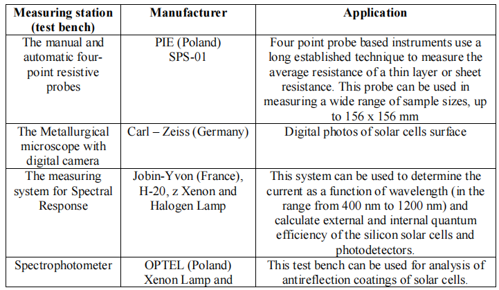
Besides the technological line for manufacturing of solar cells, which pictures have been enclosed to the following part of this article (this pictures show the chosen stations of the technological line), The Photovoltaic Laboratory of Institute of Metallurgy and Material Sciences of PAS owns the measuring stations which enable complex characteristics of crystalline silicon parameters as well as of solar cells in the individual stages of their manufacturing. The setting-up of diagnostic-measurement stations, which are being utilized to making material parameters characteristic and which are being employed in the technology of solar cells manufacturing has been presented in the table number 1.
Table. 1. The setting-up of diagnostic-measurement stations in PL IMMS PAS, which are being utilized to making material parameters characteristic and which are being employed in the technology of solar cells manufacturing.

The base material
Crystalline silicon has been the dominant material for the production of solar cells for the past 20 years and this leadership is expected to continue. Two types of crystalline silicon are used in the industry. The first is monocrystalline, produced by slicing wafers from a high-purity single crystal boule. The second is multicrystalline silicon, made by sawing a cast block of silicon first into bars and then wafers. The main trend in crystalline silicon cell manufacture is toward multicrystalline technology. For this reason all investigation in Photovoltaic Laboratory of IMIM of PAS are focused on crystalline solar cells. Until recently the base material were monocrystalline silicon 0,5 - 1 Ωcm, <100> oriented, p-type, Cz-Si wafers and multicrystalline Si, p-type, thickness of 300 μm, minority carriers diffusion length ~ produced by Deutsche Solar (Baysix). The highest losses occur during the wafering where about 40 % of Si is lost as kerf. For the typical wafer 300 μm thick at the present, the kerf loss is 180 - 200 μm. Answer to this problem is use of thinner substrates, today 300 microns thin gradually is shifting to a thickness of 100 – 130 microns. Nowadays all investigation processes are carried out using the monocrystalline base material from ITG company (Switzerland). The main difference between Baysix and ITG silicon is thickness of plates. The base material used in this study were mono Si, 200μm thick form ITG and multicrystalline Si – 200 μm thick from Deutsche Solar. The main parameters of used base material are described in table 2.
Table 2. The main parameters of silicon plates using as a base material in solar cells technology
