ABSTRACT
Metal assisted chemical etching is a promising method for fabricating high aspect ratio micro- and nanostructures in silicon. Previous results have suggested that P-type and N-type silicon etches with different degrees of anisotropy, questioning the use of P-type silicon for nanostructures. In this study, we compare processing X-ray zone plate nanostructures in N and P-type silicon through metal assisted chemical etching with a gold catalyst. Fabricated zone plates were cleaved and studied with a focus on resulting verticality, depth and porosity. Results show that for high aspect ratio nanostructures, both N and P-type silicon prove to be viable alternatives exhibiting different etch rates, but similarities regarding porosity and etch direction.
1. Introduction
Metal Assisted Chemical Etching (MACE) is a promising method to obtain deep silicon nanostructures with well-defined patterns and a high aspect ratio. There are however still questions on the optimisation of the MACE process, and different catalysts and doping types of silicons have been suggested as successful measures for a reliable process. Depending on the catalyst, which is often a noble metal such as Pt or Au, differences in etch rates might occur. The compositon of the etching solution also offers space for tuning with regards to etch direction and etch rate.
The purpose of this paper is to investigate and discern the differences and similarities of metal assisted chemical etching of nanostructures in N-type and P-type silicon. Fresnel zone plates will be used as model patterns. Similar kinetics have been studied before, but not with deterministic structures defined by EBL, nor on such a wide range of scales for each sample. The zone plate patterns utilized have structures ranging from micro to nano-scale, which offers great insight for how the etching process affects the gold catalyst for vastly different feature sizes. In the field of X-ray imaging, zone plates are a common kind of focusing optics. To obtain a small focus, zone plates with outermost features in the nanometer range are required, while the inner zones are in the order of micrometers. Other demands on the optics include a high aspect ratio or certain materials being used. Zone plates fabricated using MACE have previously been used successfully as focusing optics for X-ray imaging. This makes zone plates ideal as a model system for analysing the etching results on different length scales.
2. Materials and method
2.1. Sample preparation
N (phosphor doped, 1–5 ohm/cm resistivity) and P-type (boron doped, 1–5 ohm/cm resistivity) silicon wafers with a 100-orientation (Si-Mat) were diced into 1 cm2 and 0.5 cm2 pieces. All samples were sonicated in isopropanol (IPA) for 5 min at 80 kHz and blow dried under N2 gas flow. N and P-type silicon chips were then sorted into pairs and labelled so to ensure that the sample pairs that underwent similar sample preparation conditions would also be etched under the same conditions. This so to ensure samples could be adequately compared. Each chip pair underwent a reactive ion etch cleaning step for 5 min (20 sccm O2) to achieve a clean surface for the resist. A 90 nm resist layer, consisting of CSAR 62–9 (Allresist GmbH) diluted with anisol (1:1) was applied through spin coating at 7000 RPM for 1 min. The resist layer was baked at 150 ℃.
2.2. E-beam lithography and metallisation
The desired pattern was designed in MATLAB, and consisted of zone plates with a so-called fish bone design. These patterns have previously been identified as well suited for the MACE process. The specifics and performance of the design can be found elsewhere. The zone plates were printed in groups of 9 with supporting structures on three of the sides. Each zone plate was 150 μm in diameter with a smallest outermost zone of 30 nm. The patterning was conducted with a 50 kV electron beam lithography system (RAITH Voyager). The starting dose was approximately 120 μC/cm2. Both zone plates and supporting structures were printed using a low-current 30 μm aperture (LC30). The patterns were developed in amyl acetate (AR546, Allresist GmbH) for 1 min, followed by a 10 s soak in IPA as a stopper step to halt the development. The development process was finished with a 20 s rinse in pentane, and the samples were left to air-dry.
2.3. Lift-off
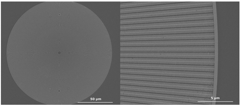
Resist was stripped from the samples using a wet chemical lift-off process utilizing sonication and the same remover solution as in previous steps. The samples were rinsed in the remover before sonicated in acetone for 10 min at 80 kHz. Samples were then transferred to fresh remover solution, and the sonication step was repeated. This cycle of sonicating in acetone and remover sequentially was repeated once but at half the time at each step. Two cleaning steps of sonication in IPA and deionized water for 10 min each concluded the lift-off process, before all samples were dried under N2 flow. An example of the resulting gold zone plate pattern is shown below in Fig. 1.

Fig. 1. SEM images of the resulting gold zone plate pattern on the silicon wafer after liftoff has been conducted. The light parts shows where gold has been deposited in the printed pattern, and the darker area is areas free of gold.
2.4. Metal-assisted chemical etching
All samples underwent a 3 min RIE step (10 sccm O2) to ensure a clean surface for the etching step. The etching solution consisted of 4.7 M HF, 0.68 M H2O2 and 0.91 M isopropanol, which should yield an etch rate for P-type silicon of 0,28 μm/minute. The solution containing IPA was chosen as it yields slower etch rate, which has been found to improve the quality of the etched structures. Three rounds of etching were performed, at 5, 7.5 and 10 min respectively. Each sample was etched individually directly after one another, and in a closed container so to assure the reaction is conducted without any light influence. The solution was mixed fresh for each etching experiment. At the end of the etching process, the samples were rinsed in DI-water before transferred to a crystallisation dish with ethanol to ensure a constant wet surface. All samples were then dried using a CPD process (LeicaEM CPD 300) to minimize the risk of any structural collapse.
3. Results
3.1. Etch rate and resulting verticality
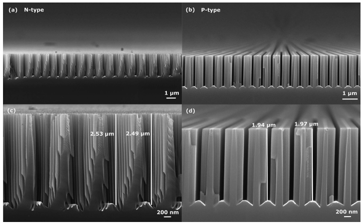
Imaging the samples with SEM revealed well defined and anisotropically etched structures of varying depths. In Fig. 2, the cross sections of both the N and P-type samples shows that the silicon has etched vertically without any larger discrepancies. At the bottom of each structure, the gold mask can be seen as a brighter area. The mask has travelled down slightly quicker towards the outermost sides of each canal. This is due to the fish bone nature of the pattern exhibiting structures of different sizes . The end of each finger will travel down slightly quicker than the wider parts responsible for the interconnects between the zones of the pattern. There is a difference in etch rate between the samples, where N-type silicon etches quicker than P-type. This is an an expected result in line with previously reported observations. Etch rates calculated from our experiments resulted in a (0.336 ± 0.004) μm per minute for N-type silicon, and (0.259 ± 0.003) μm per minute for P-type.

Fig. 2. SEM images of cross sections of zone plates of (a) N and (b) P-type silicon, etched by MACE. Images (c) and (d) show detailed cross sections with typical measurements for the etched depth profile in each case. The samples in the image are parallel processed and have both been etched for 7.5 min.
4. Discussion
In previous studies where etching results for N and P-type silicon after MACE experiments have been highlighted, there are clear differences between the two doping types with regards to porosity, etch direction and verticality. Here we discuss our findings in view of the proposed mechanism.
4.1. Etch rate and etch direction
Studying the etch rate reveals that the N-type samples consistently etch faster than the P-type counterpart. This is due to the facilitation of Si oxidation at the metal-silicon interface, due to Schottky barrier band bending . There is however no tangible difference in resulting verticality between the samples. Neither the micron sized, nor the nano structures in the sub 100 nm regime have etched at an inclined angle or with a widening of the top part of the trench. The driving mechanism of the etching has previously been suggested as a hole injection process. According to Lai et al., the process is regulated by a Schottky catalytic process. The mechanisms have been suggested to be different between P and N-type, resulting in the widened shape of the etched trenches of microstructures in P-type silicon. Further investigation into the catalytic process of MACE will be needed to thoroughly determine the reaction kinetics and what determines the etch rate fully. In any case, our results show both P and N-type silicon are suitable for nanostructure fabrication through MACE as a method.
4.2. Porosity
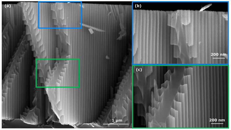
The porosity results differ little between the two sample types. There are however clear differences in porosity when the aspect of depth is discussed. In Fig. 3 porosity seems to be more prevalent towards the top of the nanostructures and less present in the deeper parts of the etched trenches.

Fig. 3. A cross section of a zone plate imaged in detail with emphasis on resulting porosity. (a) shows a grander magnification of the relevant structure. (b) depicts the top of the structures, showing a more pronounced porosity than can be seen in (c) the depths of the cleaved structures.The zone plate structure imaged was etched for 7.5 min in N-type silicon.
5. Conclusion
In this study, we have investigated the etch rate, resulting porosity and verticality for MACE of dense nanostructured patterns in N and Ptype silicon, respectively. In both cases, anisotropic etching can be seen on a sub 100 nm level feature size. For either type of silicon, satisfactory results were obtained with regards to porosity and verticality. The etch rate can serve as a determining factor of which silicon will best fit the experiment, as a higher etch rate has been consistently observed for Ntype silicon.
We observed a slight increase in porosity towards the surface level of the structures. This is however not a long range porosity, but rather a local change in surface porosity. Only the top of the structures erodes, whilst the etched nanostructures remain dense in the depths.
We did not observe a widening of the trenches for P-type samples as described by Lai et al.. Whether this is simply a result of shorter etching times in our study or not is up for debate. Further research is required to determine the nature of the chemical kinetics behind the MACE process fully, and how the hole injection kinetics adhere to the doping type of the silicon of choice in particular at the nanoscale.
下一篇: 不同HF浓度对多孔硅形成的影响