ABSTRACT: The chemical transformations taking place during many of the reactions of the Si surface have been well documented, but the in situ dynamics of the reactions remain largely unexplored even for widely used electrochemical processes such as metal-assisted chemical etching (MACE). In this work, we design both n- and p-type Si photoconductors covered with silver nanoparticles to demonstrate photoconductors’ sensitivity to the MACE process and their ability to provide in situ information about the dynamics of the reactions occurring during MACE. The experimental results show that both n- and p-type photoconductors exhibit a response to MACE that is much stronger than their response to light with an intensity of 2 mW/cm2 . The observations are further explained by a thermodynamic analysis of the relevant energy levels of the system, showing how both electron and hole injection into the conduction and valence bands by the Si/etching solution interface contribute to the photoconductors’ response and excite Si. These results clearly demonstrate a new chemical operating mode for photoconductors, showing that in addition to being sensitive to excitation by light, a photoconductor can also be excited by chemical reactions providing means to monitor the dynamics of the reactions in situ and thus also for chemical sensing.
INTRODUCTION
Metal-assisted chemical etching (MACE) as an effective method to fabricate semiconductor (especially Si) nanostructures has been widely studied over the past twenty years and is attracting more and more interest from both the scientific and technological communities.The Si nanostructures produced by MACE have been widely used in energy harvesting and storage, sensors, and biomedical technologies. In addition, inspired by the MACE reaction, plasmonenhanced nanomotors moving at the silicon/MACE etching solution interface have been developed based on the attractive plasmon resonance of noble metal, e.g., Ag and Au, nanocrystals.The MACE process is based on the highly site-selective oxidation of Si when it is brought into contact with metal nanoparticles (typically silver nanoparticles, AgNPs) and oxidants (typically hydrogen peroxide, H2O2) in a fluorine-containing solution. The oxidized products of Si can be easily etched away by a fluoride solution and thus highaspect-ratio silicon nanostructures are produced in the end. After twenty years of studies, the chemical transformations that take place during MACE have been well characterized, but the dynamics of the detailed charge transfer process taking place during the process have not been reported so far.
The Si−metal−oxidant nanosystems formed during MACE have been usually considered as microscopic and shortcircuited galvanic cells where Si serves as an anode and the metal nanoparticles serve as cathodes.This description focuses on the overall charge flow proceeding from Si to oxidants instead of detailing the role of Si energy bands in the charge transfer process. Cui et al. proposed a Schottky barrier (formed between metal and silicon) mechanism for charge transfer during MACE,which was challenged by a recent study where the oxide-assisted chemical etching was first reported. Another more widely accepted proposal is Si oxidation by the injected hole from H2O2 in the valence band. Focusing only on the valence band reactions, these descriptions, however, do not consider the role of the conduction band and related electron injection process on the charge transfer during MACE.
METHODS
Fabrication of Photoconductors.
n- and p-type Si photoconductors were fabricated on high-resistivity (>10 kΩ cm) Si wafers doped either with phosphorus (n-type) or boron (p-type). The detailed fabrication process of the samples is provided in the Supporting Information. A schematic representing the most important processing steps in the process flow for the fabricated n- and p-type Si photoconductors is presented in Figure S1. Briefly, the wafers were first cleaned and then subjected to a wet oxidation treatment to grow a thermal buffer oxide layer for doping masking. After that, the regions for metal contacts were opened and heavily doped to obtain a good ohmic contact in both n- and p-type photoconductors. For the n-type photoconductors, the n+ regions were created by diffusion doping, while for the ptype photoconductors, boron implantation was employed to create the p+ regions. Afterward, the thermal oxide was entirely removed from the front and back side of both n- and p-type wafers by BHF etching. This was followed by aluminum (Al) film deposition and patterning on the back side of the wafer. After that, the Al contacts were annealed at 425 °C for 20 min in a forming gas atmosphere. The structure of the photoconductors is schematically shown in Figure 1a.

Figure 1. (a) Schematic illustration of the structure of the photoconductors. (b) Surface SEM image of the p-type photoconductor after AgNP deposition. (c) Schematic illustration of the setup used for electrochemical measurements, using an n-type photoconductor as an example.
AgNP Deposition. The prepared photoconductors were first encapsulated by hot glue and then subjected to an AgNO3 and HF aqueous bath. Specifically, two insulated copper wires were attached to the two Al contacts of photoconductors using conductive silver paste. The two copper wires were passed through two glass tubes covered with hot glue, and the samples were insulated with hot glue apart from the around 1 cm2 front side active area of the sample that was left exposed. Then, the sample was immersed in the aqueous solution of 5 mM AgNO3 and 6 M HF for 8 min, during which the AgNPs were deposited on the active area of the sample by the displacement reaction of Si with Ag ions. After that, the sample was thoroughly rinsed with DI water and dried with nitrogen. An SEM image of the p-type photoconductor surface after AgNP deposition is shown in Figure 1b. The diameter of deposited AgNPs is around 100 nm. Hereafter, the samples with the ntype photoconductor without AgNP coating, the n-type photoconductor with AgNP coating, the p-type photoconductor without AgNP coating, and the p-type photoconductor with AgNP coating are called n-PC-planar, n-PCAgNPs, p-PC-planar, and p-PC-AgNPs, respectively.
RESULTS AND DISCUSSION
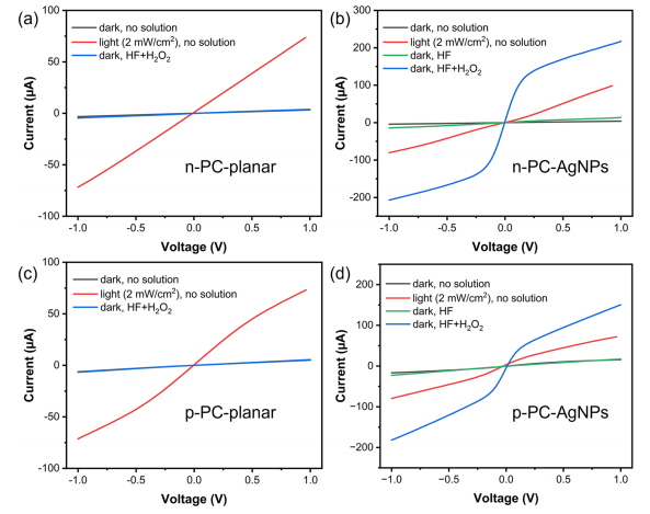
I−V measurements were performed on the above-mentioned four types of devices in the dark and under exposure to light or different solutions, and the results are shown in Figure 2. In darkness and without exposure to any solution (black lines close to zero), all of the devices exhibited an ohmic behavior but very small current (the I−V curves were straight lines with a very small slope implying a high resistance for the devices). When exposed to light with an intensity of 2 mW cm−2 (red lines), all four devices worked as photoconductors and exhibited a clear response to illumination, which was reflected by the increase of the slopes of the I−V curves. When exposed to the MACE solution (HF and H2O2, blue line) in the dark, quite interestingly, both n-PC-AgNPs and p-PC-AgNPs showed a strong response, which was seen as a significant increase of the slopes of I−V curves that was much higher than their response when exposed to light with an intensity of 2 mW cm−2 . Correspondingly, no obvious response was observed when the devices were exposed only to the HF solution without H2O2 (green lines) or when n-PC-planar and p-PCplanar were exposed to the MACE solution (blue line). In addition, no obvious response was observed when the devices were exposed only to the H2O2 solution without HF (Figure S2). Current saturation at large bias voltages was confirmed by simulations (not shown) to arise from the decreased concentration of the majority carriers near the positively biased Al contact electrode in the case of p-type photoconductors (and vice versa for n-type photoconductors).

Figure 2. Current−voltage curves of n-PC-planar (a), n-PC-AgNPs (b), p-PC-planar (c), and p-PC-AgNPs (d) in different conditions. The black lines in panels (a, c) are not clearly visible because they almost completely overlap with the blue lines.
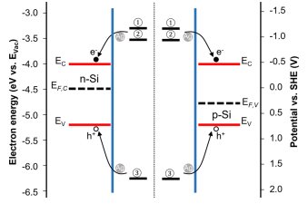
The driving force for electron transfer in semiconductor electrochemistry is always the difference between the quasiFermi levels and/or electrode potentials, albeit in the literature, the Fermi level is often approximated to coincide with the closest band edge. Furthermore, the contributions of the two energy bands to the charge carrier exchange between redox couples in the system are of rather unequal magnitude, and one of them dominates the current. The dominant contribution to the current typically comes from the band that is closer to the electrode potential of the redox couple. As shown in Figure 3, in the MACE system, the conduction band overlaps well with the oxidation reactions of Si, and the valence band overlaps well with the reduction reaction of H2O2. Therefore, for the oxidation of Si, the charge carrier exchange would be mainly expected to occur with the conduction band, and for the reduction of H2O2, it would mainly occur with the valence band. With the energy level of Si oxidation (both divalent and tetravalent oxidation) higher than the quasi-Fermi-levels of the conduction band of both the n- and p-type Si, and the energy level of the H2O2 reduction lower than the respective quasiFermi-levels of the valence band, as shown in Figure 3, the dominant charge carrier exchange between the energy bands and redox couples in the MACE system would be electron injection from the oxidation of Si to the conduction band and hole injection from the reduction of H2O2 to the valence band for both n- and p-type photoconductors. In addition to thermodynamics, which determines the direction of the reaction, kinetics is also an important factor to be considered in the charge carrier transfer process. AgNPs as noble metal nanoparticles, which have been widely used as highly efficient catalysts for various (electro)chemical reactions, could decrease the activation energy of the reactions due to their high catalytic activity and thus significantly enhance the kinetics of the charge carrier injection processes.

Figure 3. Energy diagram showing the absolute positions of the Si conduction-band minimum (EC), the Si valence-band maximum (EV), and the calculated Fermi levels of n-type Si (EF,C) and p-type Si (EF,V) used in this work. The electrode potentials vs SHE of reaction ①: Si + 6F− + 2H+ → SiF6 2− + H2 + 2e−, ②: Si + 6HF → SiF6 2− + 6H+ + 4e−, and ③: 2H2O2 + 4H+ + 4e− → 4H2O are also shown. The charge carrier transfer between Si energy bands and redox couples is schematically shown by the arrows.
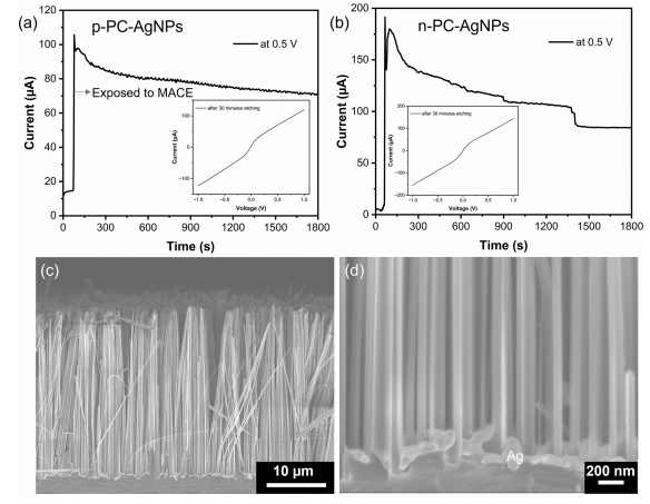
To investigate the response of the device to the MACE process in the longer term, we measured the change of current at a bias of 0.5 V when p-PC-AgNPs (Figure 4a) and n-PCAgNPs (Figure 4b) were exposed to the etching solution and etched in the solution for 30 min in the dark. When the devices were exposed to the MACE solution, a sharp increase in current was observed from both devices due to the strong chemical excitation of the devices during MACE. The current gradually decreased with time, mostly due to mass transport limitations for the etching and/or the increased recombination when more surface area was exposed when the etching proceeded inside of Si. The I−V curves of the photoconductors measured in the MACE solution in the dark after the 30-min etching are shown as insets in Figure 4a,b, showing that even after the long etching, the main features of the I−V characteristics under exposure to MACE remain unchanged. The cross-sectional SEM images of p-PC-AgNPs after the 30- min I−t measurements are shown in Figure 4c,d. Si nanowire arrays with a diameter of around 100 nm and a length of 28 μm were produced during the etching. The high catalytic activity of AgNPs is clearly observed in Figure 4d as the Si only below the AgNPs was selectively etched, also highlighting why no obvious response was observed from the photoconductors without AgNP coating when exposed to the etching solution.

Figure 4. Current−time curve of p-PC-AgNPs (a) and n-PC-AgNPs (b) when exposed to the MACE solution in the dark. Insets are the I−V curves of the devices measured in the MACE solution in the dark after 30 min of etching. (c, d) Cross-sectional SEM images of p-PC-AgNPs after 30 min of etching.
CONCLUSIONS
In summary, we have used both n- and p-type Si photoconductors coated with AgNPs to in situ probe the dynamics of the surface chemical reactions taking place during metalassisted chemical etching of silicon. The I−V and I−t results show that both types of photoconductors exhibit a strong response to the MACE process. A quantitative thermodynamic analysis was shown to be consistent with the observed dynamics of MACE. These results unambiguously confirm that both electron and hole injections into the conduction and valence bands by the Si/etching solution interface are involved during MACE and result in a chemical excitation of Si that can be monitored by the photoconductor. Our work, therefore, demonstrates that photoconductors as semiconductor devices can be chemically excited providing significant general insight into semiconductor electrochemistry. While photoconductors have been widely used for light detection, the chemical excitation of photoconductors reported here implies that they can also be used to probe the dynamics of the chemical reactions in situ and thus also for chemical sensing.
上一篇: 不同HF浓度对多孔硅形成的影响