The pinhole-free silicon oxide (SiOx) layer grown using dissolved ozone in deionized water (DI-O3) is demonstrated. An ultrathin SiOx layer of thickness 1.53 nm±1.5% is grown on silicon wafer using 7 ppm DI-O3. A four-step methodology, including 25 wt% aq. tetramethylammonium hydroxide (TMAH) solution at 80 °C, is employed to magnify the pinhole signatures in the underlying silicon and visualized with dark-field optical microscopy (DFOM) and scanning electron microscopy (SEM). The DFOM images show spots on the surface of wafer that originate from airborne particles, contamination, etc. SEM images reveal the absence of etch pits in silicon even after etching of SiOx/silicon in TMAH for 300 s. The minority carrier lifetime and interface states density in AlOxcapped SiOx/Si structure are ≥2 ms at carrier density of 1 x 1015 cm-3 and less than 2 x1011 cm-2 eV-1 , respectively.
1.Introduction
Though crystalline silicon (c-Si)-based devices hold≈90% of the market share for solar photovoltaic (PV), efforts are being made to reduce their levelized costs of energy (LCOE) for grid parity realization. Reduction in LCOE of PV devices can be achieved by lowering their production cost and increasing their conversion efficiency. In order to achieve high-efficiency potentials, it is necessary to minimize surface recombination-induced losses of photogenerated charge carriers.The scientific community has widely used surface passivation schemes involving thin dielectric layers to minimize such losses. SiOx is the most intriguing dielectric material which has been implemented as standalone or in stack forms with other materials (SiNx, AlOx, etc.) for tunneling as well as passivation purposes. The most influential and mass production technique to grow SiOx layers is thermal oxidation. However, requirement of high processing temperature and extended hours for single run made thermal oxidation undesirable considering production cost and throughput. Other important concerns at high temperatures are survivability of bulk minority carriers’ lifetime of wafer and contact metals. Hence low-temperature oxidation techniques such as plasma enhanced chemical vapor deposition (PECVD) and nitric acid oxidation of silicon (NAOS) have gained popularity. However, PECVD is suitable only for single-sided SiOx deposition at a time that introduces an extra processing step. SiOx formed with NAOS technique needs high-temperature (≈1100 °C) annealing for getting good surface passivation. Besides this, nitric acid is a hazardous chemical itself and known for acute lung injury in case of exposure.
Furthermore, the existence of pinholes in thermal, PECVD, and NAOS-based oxides manifests adverse effects on performance of solar cells. For example, pinholes in the passivation layer (e.g., in passivated emitter and rear cell (PERC) cells) lead to direct exposures of silicon surface to the contact metal (e.g., aluminum) that create local recombination centers and thus increase the effective recombination velocity. In addition, the presence of pinholes in the dielectric layer in back-contact back-junction (BC-BJ) solar cell designs results in a local shunt that reduces their performance. In metal–insulator– semiconductor (MIS) solar cells, intimate contact of metal with the semiconductor through pinholes makes Schottky contact there, that causes additional spreading resistance in the structure. The saturation current in such a case depends on the quality of the Schottky contact and pinhole diameter.
2. Results and Discussion
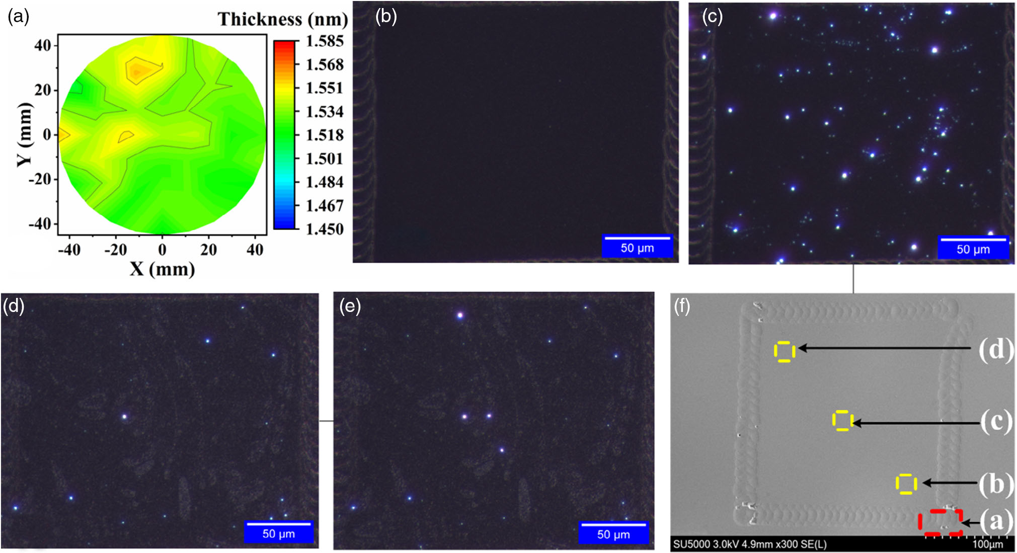
Figure 1a shows the thickness variation in DI-O3 oxide on silicon which is estimated as 1.53 nm ±1.5%. The DFOM images of one square on one wafer, processed with the aforementioned methodology, are displayed in Figure 1b–e. Figure 1b shows the absence of any “spots/holes” in the laser-marked and chemically cleaned wafer, which confirms that initially the wafer was free from defects and contamination. However, after the growth of DI-O3 oxide, some spots can be visualized on the surface of the square under discussion, as depicted in Figure 1c. Variations in the spot sizes created uncertainty if they are really pinholes. To clarify such uncertainty, the DFOM imaging of the same square was carried after TMAH etching and is shown in Figure 1d. It can be noticed that many of the spots are swept out. If all of them are pinholes, the corresponding etch pits/inverted pyramids should be created in the underlying silicon. Such findings suggest that all spots cannot be assumed as pinholes. Furthermore, Figure 1e shows that the spots, visualized after TMAH etching (i.e., in S-3), were observed at random positions along with the varied number of counts after final HF dip (i.e., in S-4).

Figure 1. a) Thickness uniformity (.53 nm + 1.369 in the grown si0, laver.50x zoom DfOM image ofthe marked square after b) laser marked anddean, that is,step-1. ) Dl0,assisted growth of si0,layer, thatis, step2. d) TMAH etching of wafer, that is, step3 and e) hnal Hf etch, that is, step4f) The SEM image ofthe same inspected square, wherein the red and yellow marked areas are magnifed in figure 2.
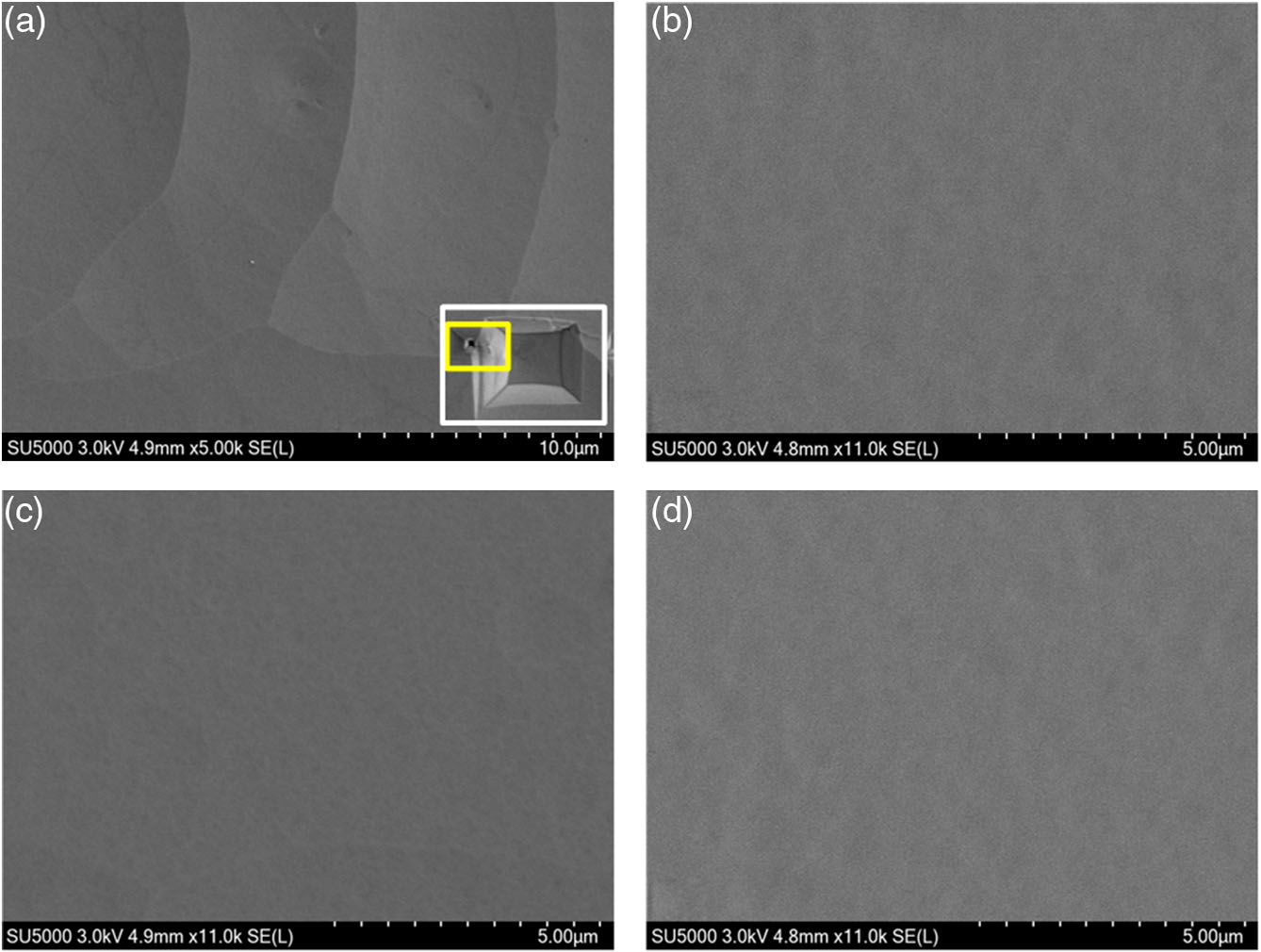
A recent study revealed that the edge length of the maximum number of etch pits in silicon, created by 15 wt%aq. TMAH etching of silicon through pinholes in SiO2 for 300 s, is ≈250 nm. Though etch rate is reported higher for 25 wt% aq. TMAH at 80 °C than 15 wt% aq. TMAH at 90 °C, roughly the same size or even wider etch pit is expected in the present case if pinholes exist. For example, one can clearly see the etch pits on the laser-scribed lines in Figure 1f. There exist smaller etch pits on the same marked line as well, for example, within the red highlighted portion in Figure 1f that is magnified in Figure 2a. Such etch pits are due to TMAH etching of the silicon through the pinholes in DI-O3 oxide that is unable to coat some parts of silicon damages created by laser marking to create squares. As the whole silicon wafer went through TMAH etch, there would be etch pits if there were pinholes in DI-O3 oxide on the laser-marked lines or the inner part of the laser-marked squares. Figure 2 depicts a comparison between the laser-scribed line versus the inner part of the marked square (i.e., the area grown with DI-O3 with no laser marking). In Figure 2a, the presence of etch pit/s can be clearly seen on the laser-scribed line. The inner part of the marked square is further investigated at higher magnifications and at random locations highlighted as yellow portions in Figure 1f. The SEM images of those portions are shown in Figure 2b–d, which clearly depict the absence of pinholes. A comparison of Figure 2a–d clearly shows that etch pits are present only on the laser-scribed line.

Figure 2. a) For illustration purposes, the magnified view of the red square in Figure 1f where a smaller etch pit is shown in yellow square and bigger etch pit is in white square. b–d) the SEM imaging carried out at different locations, which were highlighted yellow in Figure 1f.
The above results suggest that DI-O3 oxide is free of pinholes. Such results are in stark contrast with its counterpart, that is, NAOS-grown oxide layers, where the pinhole density has been estimated as 5x109 cm-2. This is because the oxide grown by NAOS is in the form of dense islands, which makes it highly nonhomogeneous. The space between the islands does not get oxidized, that resulted in the formation of pinholes in the grown oxide.Ozone-based oxide, on the other hand, is very conformal even at the atomic level. Its growth occurs in a layer-by-layer manner, which produces a homogeneous oxide layer.The repeatability of the present experiment is ensured by processing one additional wafer under same conditions and at different time, which provided the same results. The findings of the present work make DI-O3 oxide a strong candidate for implementation in c-Si PVs and beyond. Above results also inferred that imaging of pinholes/etch pits with DFOM should be used in conjunction with other high-resolution techniques including SEM, rather than by itself, as the spots observed in Figure 1b–e are due to adsorption of particles/contaminations on the surface of wafer, which could lead to inaccurate conclusions. One possible origin of such airborne particles/contaminations may be occupancy in the lab during measurements.
3.Experimental Section
In this experiment, p-type boron doped 3 in mirror-polished CZ Si wafers of resistivity ≈ 0.005 Ω cm with <100> orientation were used. This section gives an overview of the experiment performed. For more details, readers may refer to the supplementary file.
In the first step (S-1), six squares, each of size 250 μm x 250 μm (which was the field of view for the used DFOM in this experiment), were marked at different locations on the wafer using a 20 W ytterbium fiber laser at a power of ≈ 25%. The squares marked by laser ensured that subsequent inspections of pinholes took place on the exact same location. The wafer was then cleaned and etched for laser-induced damages in 25 wt% aq. TMAH solution for 5 min. at a temperature of 80 °C. The wafer was cleaned and dried with N2 gun.
4. Summary
In summary, we investigated the existence of pinholes in the DI-O3-grown oxide layer. Consistency in the experiment is established by adopting a systematic approach wherein DFOM imaging was carried out at the same location on the wafer after every step and then inspected by SEM. Though DFOM imaging initially identified some spots, which appeared like pinholes; those spots turned out to be airborne particles and/or contamination through the subsequent investigation by SEM. The SEM images in the present work validated the absence of etch pits in the silicon that emphasized that the grown DI-O3 oxide is free of pinholes. The experiment yielded the same results on two wafers (i.e., a total of 12 squares), processed at different times, which demonstrated its repeatability. Additionally, this investigation revealed that DFOM and SEM should be used in tandem, rather than individually for more conclusive outcomes. The quality of the grown oxide is revealed in terms of measured minority carrier lifetime and Dit.
上一篇: 金属辅助化学蚀刻对硅光电导体的化学激发
下一篇: 低温下在硅晶圆上单步碳化硅异质外延