ABSTRACT
A single step growth approach for wafer-scale homogeneous cubic silicon carbide (3C-SiC) heteroepitaxy, using chemical vapour deposition (CVD), on a silicon (Si) substrate is demonstrated. Residual biaxial tensile strain causing a wafer bow is eliminated in the 3C-SiC epilayer via in-situ defects engineering and heteroepitaxy at reduced temperature. Thermal mismatch between the 3C-SiC epilayer and substrate is minimised by a substantial reduction of growth temperature, down to ~1000 ◦C. Heteroepitaxy of high quality, fully relaxed 3C-SiC epilayers with minimal wafer bow is demonstrated, made possible by careful process optimisation. Unusually very high growth rate of 3C-SiC of > 10 µm/hr is achieved. At the same time the epilayer is free from any other silicon carbide (SiC) polytype inclusions. Moreover, the reduced growth temperature unlocks the ability to deposit high quality 3C-SiC epilayers within traditional Si-based cold walled CVD reactors, enabling the growth of such thin films on unprecedently high volumes and wafer diameters up to 300 mm and above.
1. Introduction
Silicon carbide (SiC) is a wide bandgap compound semiconductor which shows high potential for the ongoing electrification of the world and creation of disruptive technologies in sensors, microelectromechanical systems (MEMS) and harsh environment electronics and optoelectronics. The next generation of power electronics can contribute in suppressing climate change by improving the efficiency of electric power conversion, which is applicable to a range of industries and social infrastructures . The high electric field breakdown and low switching losses of SiC make it ideal for high voltage and high frequency applications such as those found in electric vehicles. Also SiC possesses other excellent material properties at room-temperature such as high thermal conductivity (360 W m-1K-1), high hardness (9.3 Mohs hardness), and resistance to all wet and gaseous chemical etchants. It is not susceptible to damage from various forms of radiation as well. Semiconductor devices fabricated from SiC can operate at very high temperatures (>600 ◦C) and in harsh environments. These properties make it ideal for use in various applications beyond power electronics including microwave, harsh environment sensors, MEMS and biomedical devices. Also, relaxed cubic SiC, with a lattice constant of 0.436 nm, grown on a silicon (Si) substrate, is ideal virtual substrate for subsequent epitaxy of other scientifically and technologically important materials such as gallium nitride (GaN), aluminium nitride (AlN), boron nitride (BN), boron arsenide (BAs), Diamond and various 2D materials, including graphene, and thus allows their integration with Si . Successful device technology is greatly dependent on the wafer/substrate and epitaxial material quality.
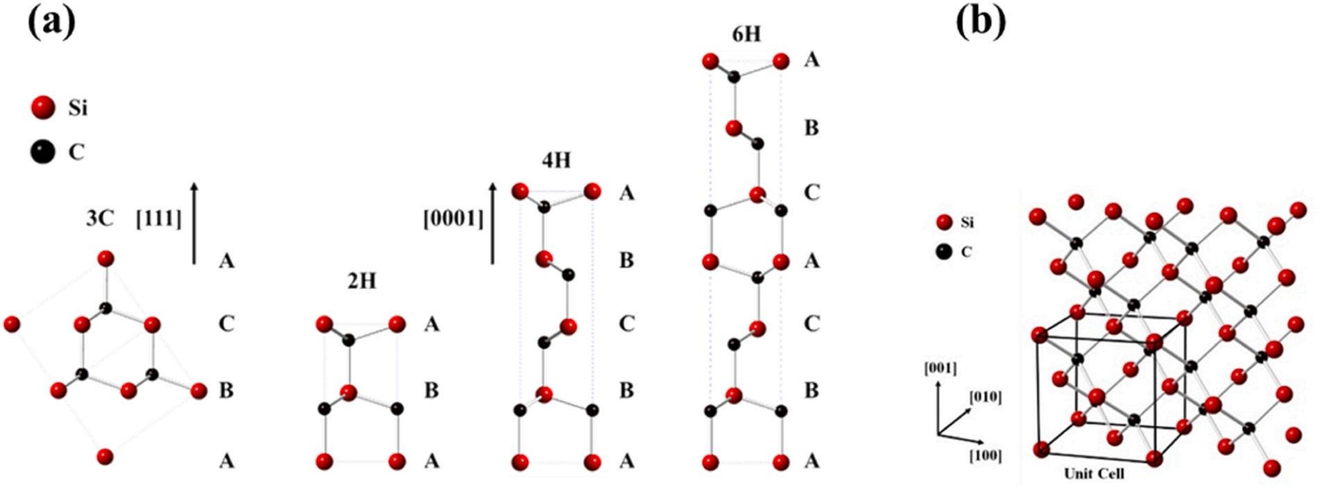
SiC exists in over 250 different crystalline forms called polytypes, see Fig. 1 . The hexagonal structured 4H-SiC dominates the SiC market due to the availability of crystalline wafers up to 150–200 mm diameter and well-developed homoepitaxial growth processes. While 4H-SiC is available in commercial applications, such as power devices and substrates for GaN and other III–V materials, 4H-SiC wafers are extremely expensive and subsequent homoepitaxy requires dedicated hot-walled chemical vapour deposition (CVD) reactors operated at very high temperatures over 1650 ℃, which leads to high operating and maintenance costs. Nevertheless, 4H-SiC epilayers and substrates still contain various defects and polytypes inclusions.

Fig. 1. a) Unit cells of SiC polytypes: 3C-SiC, 2H-SiC, 4H-SiC and 6H-SiC (left to right). (b) Cubic crystal structure of 3C-SiC showing unit cell.
The first synthesis of 3C-SiC on Si(001) substrate was reported by Spitzer et al. in 1959, over 60 years ago, and much work has been carried out to improve the quality of the 3C-SiC epilayers since. In that pioneering work, thermal CVD process with just methane diluted in argon was used to convert the surface of a Si wafer, via diffusion, into some form of graded and non-uniform SiC thin film at a temperature of 1300 ◦C. It took decades for another major step to happen towards the growth of 3C-SiC thin films. Inspired by the similarities of the crystal structures between 3C-SiC layers and Si substrate, and the maturity of Si wafer technology, Spitzer’s work overlooked the fact that the considerable difference between both their lattice parameters and thermal expansion coefficients (TEC); the disparities that are responsible for the large number of defects at the 3C-SiC/Si interface that, as the growth continues, also propagates through the epilayer to the surface. In 1983 Nishino et al. implemented a three step (cleaning, carbonisation, and growth at ~1350 ◦C) CVD process for improved quality crystalline growth. Through this process, that included a buffer layer (carbonisation layer), some graded SiC seed layer would be deposited, on top of which the succeeding 3C-SiC epi layers would be grown. The inclusion of a SiC seed layer dramatically improves the crystal structure of the 3C-SiC and helps to reduce wafer bow caused by thermal mismatch. Having been considered an improvement to Nishino’s three step process, in 2009 Chen et. al. introduced a four-step growth technique with no cooling periods in between, in a low pressure CVD reactor in which a (post-carbonisation) diffusion step was added to the conventional three step process. This modified four-step process helps producing 3C-SiC epitaxial layers of improved crystal quality and reduces the formation of voids at the interface, which can form due to the out-diffusion of Si from the substrate.
2. Materials and methods
2.1. Epitaxial growth
3C-SiC epilayers of thicknesses up to ~1 µm were grown on on-axis 100 mm diameter 525 µm thick Si(001) wafers within an industrial type Si based ASM Epsilon 2000 RP-CVD cold wall system, with the capability to grow on up to 200 mm diameter wafer. It consists of a cold-walled quartz chamber, which limits an upper growth temperature to ~1200 ◦C and which makes achieving highly crystalline 3C-SiC a challenge. However, high throughput of these machines and significant reduction of deposition on the chamber walls would allow mass production of low-cost 3C-SiC/Si epi wafers utilising the existing network of Si-foundries. The C to Si ratio was controlled through the ratio of C to Si gaseous precursors injected into the growth chamber at reduced pressure below 200 Torr. Dichlorosilane and trimethylsilane were used as precursors. Growth rates of over 10 µm/hr were obtained. The Si wafer was loaded into the CVD growth chamber at 900 ◦C, as shown in Fig. 2b. Then the temperature was rapidly raised up to ~1000 ◦C at which native silicon oxide was thermally desorbed from the Si surface. Immediately after that the growth of 3C-SiC commenced.

Fig. 2. Heteroepitaxy of 3C-SiC on Si. (a) State of the art multi-steps 3C-SiC heteroepitaxy. (b) Novel reduced temperature heteroepitaxy growth process showing simplified steps and dramatically shorter processing time.
Initial growth processes for 3C-SiC were carried out at temperatures of ~1200 ◦C. To suppress the out-diffusion of Si and to create a seed layer for the subsequent epitaxy of 3C-SiC a silicon carbon alloy (Si1− xCx) buffer layer was deposited with approximately 1 % C composition. In contrast to well established carbonisation buffer, see Fig. 2a, which creates some graded Si1− xCx layer of poor quality and not even monocrystalline in the most cases, we used to innovation and introduced a defect free Si1− xCx alloy epilayer lattice matched to Si, which maintains the same crystallinity as Si substrate. As the growth process was further optimised, the deposition temperature was reduced to ~1000 ◦C at which point the out-diffusion of Si could be suppressed through optimising the C/Si ratio in the growth phase and as a result the Si1− xCx buffer layer was found to be unnecessary and a simplified process could be used, as shown in Fig. 2b. However, it could indeed be used as a seed layer for traditional high temperature 3C-SiC heteroepitaxy on Si.
3. Results and discussion
3.1. C/Si Ratio
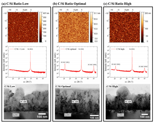
After the selection of appropriate precursors, the C/Si ratio must be adjusted in order to grow a high quality 3C-SiC compound epilayer, but not a Si1− xCx alloy or SiC compound with high density of interstitial Si or C defects. Correct C to Si ratio is absolutely essential to obtain SiC compound of any polytype including 3C-SiC. Thermal decomposition of any Si or C precursor depends on the bonding energy of a particular precursor molecule and therefore could create more or less Si or C atoms emerging on the substrate’s surface. A 3C-SiC epilayer grown under optimum growth conditions exhibits the lowest surface roughness and the highest crystal quality. Characterisation results from samples growth with reduced, optimal and increased C/Si ratios can be seen in Fig. 3. Non-optimal growth conditions produce very high surface roughness implying poor island growth mechanisms with high levels of interstitials, however, at optimal C/Si ratio a very low RMS of ~3 nm can be achieved, which results in a mirror-like surface of the 3C-SiC/Si(001) epi wafer, see Fig. 5.

Fig. 3. Influence of C/Si ratio on the properties of 3C-SiC epilayers showing surface morphology with AFM maps, crystallinity with HR-XRD coupled scans and structure and defect formation in X-TEM micrographs for low, optimal and high C/Si ratios.
3.3. Crystallinity, state of strain and defects
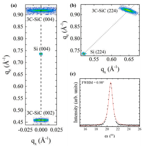
A typical HR-XRD RSMs obtained on a high quality, i.e. grown with optimal C/Si ratio, 3C-SiC/Si(001) epi wafer are shown in Fig. 4. They proof that the 3C-SiC epilayer is free of any tilt relative to the Si(001) substrate and is under only a slight residual tensile strain of < 0.1 %. Analysis of the RSMs shows both in-plane and out of plane lattice constants of the 3C-SiC are the same, i.e. ~0.436 nm, indicating the epilayer is fully relaxed. Moreover, Fig. 4c shows ω rocking curve, which was obtained around the 3C-SiC(002) Bragg peak for the 300 nm thick epilayer and its FWHM found to be 0.98◦. The broadening of the peak appears due to presence of defects in the epilayer, but it is comparable to the values obtained in 3C-SiC layers grown at higher temperatures. Growing thicker epilayer would decrease the defect density and reduce the FWHM of the film. It is necessary to point out that full relaxation of the 3C-SiC epilayer is achieved in very thin and just 300 nm thick epilayer.

Fig. 4. HR-XRD RSMs. (a) Symmetrical (004) and (b) asymmetrical (224) RSMs of a 300 nm thick 3C-SiC/Si(001) epi wafer grown using an optimal C/Si ratio. (c) FWHM of the 3C-SiC(002) Bragg Peak. Symmetrical RSM indicates absence of 3C-SiC epilayer tilt, while the asymmetrical RSM clearly visualise absence of substantial residual strain in the 3C-SiC epilayer.
3.6. Thickness Uniformity
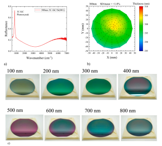
Superior 3C-SiC epilayer’s uniformity across a full wafer is demonstrated as well, which is essential for mass production and high yield. Fig. 5a shows FTIR reflectance spectrum for a 300 nm thick 3C-SiC epilayer. Fig. 5b shows 2D thickness map of 3C-SiC epilayer with thickness uniformity of < 1.5 % across 100 mm wafer. Epi wafers of varying 3C-SiC epilayer thickness from 100 up to 800 nm exhibits superior uniformity visible due to colour variation of wide band gap 3C-SiC epilayer grown on Si, as shown on Fig. 5c.

Fig. 5. Wafer uniformity. (a) FTIR reflectance spectrum for a 300 nm thick 3C-SiC epilayer. (b). Wafer uniformity of a 100 mm 3C-SiC epi wafer showing uniformity of < 1.0 % across 90 % of the wafer diameter. (c) Epi wafers of various 3C-SiC epilayer thickness exhibits superior uniformity visible due to colour variation of wide band gap 3C-SiC epilayer grown on Si.
4. Conclusions
In conclusion, the novel approach reported here has created a technology, which allows not only wafer scale homogeneous 3C-SiC heteroepitaxy on on-axis Si(001) wafer, but also beyond state of the art 3C-SiC epitaxial material quality. Moreover, the process is much simpler, faster, cheaper, substantially less energy consuming and consists of just a single growth step comparing to traditional multi-steps. High quality 3C-SiC epilayers can be grown at low temperatures down to ~1000 ◦C without the requirement for carbonisation or other buffer layers. High growth rates of above 10 µm/hr are achievable, which would enable the growth of very thin and very thick epilayers from 10’s nm up to 10’s µm covering a wide range of applications. High crystallinity, low surface roughness, minimal wafer bow and excellent uniformity both across each wafer and from run to run is achieved with this technique. Crucially the process can be run in a Si-based cold-walled CVD system. The process is comparable to standard Si epitaxy and offers 3C-SiC growth at a similar cost point and scale. Various other technologies are also unlocked within such reactors and reduced growth temperatures, including selective epitaxy on SiO2 patterned substrates, blanket growth on SOI wafers and integration with other technologically important Group IV semiconductors.