Abstract: Detecting subsurface defects in optical components has always been challenging. This study utilizes laser scattering and photothermal weak absorption techniques to detect surface and subsurface nano-damage precursors of single-crystal silicon components. Based on laser scattering and photothermal weak absorption techniques, we successfully establish the relationship between damage precursors and laser damage resistance. The photothermal absorption level is used as an important parameter to measure the damage resistance threshold of optical elements. Single-crystal silicon elements are processed and post-processed optimally. This research employs dry etching and wet etching techniques to effectively eliminate damage precursors from optical components. Additionally, detection techniques are utilized to comprehensively characterize these components, resulting in the successful identification of optimal damage precursor removal methods for various polishing types of single-crystal silicon components. Consequently, this method efficiently enhances the damage thresholds of optical components.
1. Introduction
Optical component processing typically involves grinding, polishing, shaping, and other abrasive-based processing technologies. These processes generate small brittle/plastic cracks, scratches, and other physical defects on the surface of the components. These defects not only affect the mechanical properties of the optical element, but also greatly impact its optical properties. Additionally, residual chemical contamination from polishing abrasives and other chemical contaminants can cause laser-induced damage in high-energy/highpower laser systems, resulting in optical component failure. In high-energy laser systems, cracks, contamination, and other factors that cause laser-induced damage to optical elements constitute damage precursors. The distribution characteristics of weak absorption on the surface of fused silica optics post-treated with different processes and 355 nm laserinduced damage properties were investigated by Shi et al. The correlation between defects with different absorption levels and the damage performance of fused silica surfaces was systematically investigated. It is shown that there is a significant correlation between the density of defects with absorption above 2 ppm and the damage performance. Feng Shi studied the evolution of several nanoscale damage precursors in shallow IBE, and found that IBE can eliminate the polished redeposited layer and weaken the surface densification. It is important to determine the intrinsic properties of nanoscale damage precursors in terms of surface laser damage resistance. Damage precursors originate from the processing, handling, coating, and other processes of optical components. Therefore, it is necessary to monitor and control damage precursors throughout the entire processing of optical components to ensure that they meet the requirements of high-energy laser systems. Silicon-based materials are widely used in infrared thermal imaging systems due to their good spectral properties in the mid-infrared region. In high-power continuous laser systems, silicon-based materials are commonly used as cavity mirrors, mirrors, and other optical components due to their excellent integrated thermal performance ratios and midinfrared optical properties. The quality of the mirrors directly determines the performance of the laser system. With the development of high-power lasers, the lenses in laser systems need to withstand higher and higher power densities, and the most important limiting factor for the performance of the lenses is the damage precursor.
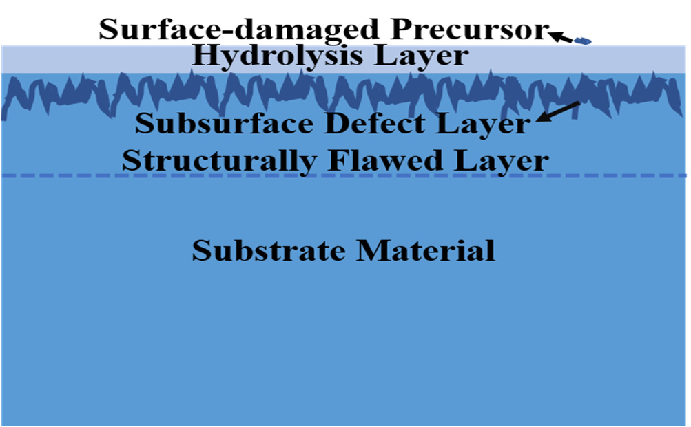
During the grinding and polishing of silicon lenses, monocrystalline silicon, being a brittle material, is prone to cracks, impurities, and other defects. Figure 1 illustrates the common defect distribution of optical materials after grinding and precision polishing. Surface and subsurface cracks, as well as impurity metal elements, may be present. These defects can be suppressed as the level of processing increases, and a layer of hydrolysis forms below the surface of the element. In brittle materials such as monocrystalline silicon, the hydrolysis layer is a layer with a refractive index comparable to that of silicon, but amorphous. Beneath the hydrolysis layer is a layer of subsurface crushing defects, which includes many scratches and cracks due to grinding and polishing, as well as a layer of defects enriched by polysilicon. Further below is a structural defect layer brought to the substrate by the grinding and extrusion process.

Figure 1. Surface defects and subsurface defects in single-crystal silicon components after processing.
2. Experimental
In our study, monocrystalline silicon optics were selected for each of the three different processing processes. All monocrystalline silicon crystals have an orientation of 100, a diameter of 50 mm, and a thickness of 5 mm. Bonnet polishing (BP) allows for uniform polishing over large areas and improves the surface finish of optical elements, but for high surface roughness and raised defects, multiple passes may be required to achieve the desired smoothness. However, for defects with high surface roughness and raised surfaces, multiple polishing passes may be required to achieve the desired smoothness. Chemical– mechanical polishing (CMP) is capable of treating surfaces of various shapes and edges, and is effective in removing small defects such as scratches and oxidized layers. However, the polishing process is more complex and requires control of the concentration, flow rate and time of the polishing solution. Magnetorheological polishing (MRF) can be performed on surfaces with unconventional shapes such as spherical and aspherical surfaces. However, the preparation of the polishing solution is more complicated and requires the configuration of special magnetorheological fluids. We provide the corresponding processes for each single-crystal silicon optical element in Table 1.

Table 1. Three sample-polishing processes
We use two different etching methods to etch damage precursors on the surface of optical elements. The first is a dry etching technique, for which we choose sulfur hexafluoride gas (SF6) and helium (He) as etching gases for the etching process. In the etching process, in general, increasing the gas flux ratio can increase the ion density and particle energy, thus increasing the etching rate. However, a too high gas flux ratio may lead to an increase in the collision between ions and thus decrease the etching rate. In addition, the etching rate increases with increasing pressure in the RIE process, and gas molecules collide with active particles in the plasma to produce an etching reaction. Increasing the pressure increases the concentration of gas molecules and the frequency of collisions, thereby increasing the etching rate. However, when the pressure is too high, the collision frequency in the plasma may be too high, resulting in the saturation or reduction of the etch rate, and possibly even “over-etching”. In addition, an increase in etching time leads to deeper etching, but this relationship depends to some extent on the etching gas used, the process parameters, and the material being etched. Therefore, based on the above analysis, we chose the following three research programs to study the dry etching process, and the specific etching process is shown in Table 2.

Table 2. Dry etching parameters.
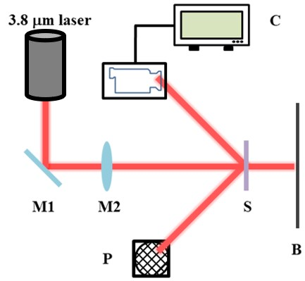
For the characterisation of the final damage test, we used the optical path shown in Figure 2. The laser outputs a 3.8 µm laser, which is focused by a lens and then irradiates the optical element. Prior to the laser damage threshold test, the laser output power and spot size were measured, the sample test spot was placed in the laser light path and irradiated using individual laser pulses of different energy densities. For each selected pulse energy, at least five test points were irradiated and recorded, and the actual pulse energy used for each test point was recorded using a beam diagnostic device. The condition (damaged or undamaged) of the sample after laser irradiation was also recorded. This test was repeated for other pulse energies. The range of pulse energies used should be wide enough to ensure that the minimum energy value will not cause damage to any of the sample test points. The maximum energy value is capable of damaging every sample test point, and damage threshold data are obtained using the damage probability method.

Figure 2. Schematic diagram of the damage test light path. The laser is 3.8 µm, M1 is an all-reflective mirror, M2 is a focusing lens set, S is a sample, C is an online damage-monitoring CCD, P is a re- flected light collection energy meter, and B is a transmitted light co.
3. Result and Discussion
Scattering test techniques enable the detection of micro and nano-level surface de.fects of optical components,. As shown in Figure 3, the bonnet-polished sampleFigure 3a) exhibited numerous scattering points, and the surface quality was poor, withmore pockmarks and scratches. The CMP-polished sample (Figure 3b) also had morescratches and pockmarks on the surface, but the number of pockmarks was significantlyreduced compared to the bonnet-polishing process. In Figure 3c, the number of scratchesin the MRF-polished samples is significantly lower than that in the CPM-polished samples,and the number of pockmarks is less than that of the previous two processes, with a signifi.cant improvement in the surface quality of the samples. By comparing these three processeswe conclude that the yRF process can effectively remove scratches and pockmarks on thesurface of the sample, and repair the roughness and surface shape of the sample.

Figure 3. Scattering test plots of samples from different polishing processes. (a–c) Bonnet-polishing process, chemical–mechanical polishing process, and magnetorheological polishing process, in that order.
Figure 4 presents the photothermal weak absorption test results of samples withdifferent polishing processes. The photothermal weak absorption technique enables thedetection of subsurface defects ofoptical elements. As shown in Figure 4, the distributionof subsurface defects of bonnet-polished samples is more extensive and covers a largerarea. This distribution is mainly due to the bonnet-polishing process, which uses flexiblebonnets and abrasive materials to smooth out scratches or defects on the surface of theoptical element. However, craters and deep scratches cannot be removed, resulting in a large area of weak absorption test results. This also explains the reason for the highnumber of pockmarks in the scattering test. CMP polishing involves the addition olabrasive materials in the chemical solution to polish the optical element. However, thepolishing solution contains elements such as cerium, which introduces metal elements andresults in very highly weak absorption values. The MRF polished samples have fewersubsurface defects compared to the previous two processes, and their distribution range issmaller than that of the bonnet-polished samples. Table 4 provides the specific values ofweak absorption for these three polishing pmcesses.

Fig4
4. Conclusions
Through the implementation of a laser-scattering test and the photothermal weakabsorption technique, we have effectively established a correlation between damage precur.sors and the resistance of materials to laser damage. In addition, we employed photother-mal absorption level as a crucial parameter to determine the damage resistance thresholdof optical elements. In this study, we investigated the damage precursors of samples withdifferent processing techniques, using the laser-scattering test and photothermal weakabsorption test to compare the characteristics of different processing techniques. Followingthat, we utilized dry etching and wet etching techniques to effectively eliminate the damageprecursors. Subsequently, these precursors were characterized using a range of testingtechniques. We successfully obtained optimal damage precursor removal methods for polishing different types of single-crystal silicon components and determined the relationshipbetween the effects of different damage precursor removal methods on damage perfor.mance. These findings have the potential to significantly enhance the damage threshold ofoptical components.
上一篇: 氧化石墨烯分类与标准化
下一篇: 电化学方法实现的纳米多孔硅材料及其应用