ABSTRACT
Crystal orientation plays a crucial role in the performance of Sb2S3 thin-film solar cells (TFSCs). Among various deposition techniques, vapor transport deposition (VTD) stands out as a viable technique for producing scalable and uniformly deposited thin films, particularly in the solar industry. This study explores temperature-modulated VTD-Sb2S3 deposition to enable efficient carrier transport in photovoltaic cells. In the VTD process, the deposition temperature is altered between 480℃ and 540℃. XRD, SEM, EDS, and AFM techniques are employed to obtain the characteristics of the Sb2S3 thin films at varying temperatures and evaluate critical features like crystal structure and orientation, surface morphology, composition, and roughness. The prominent crystal orientation changes from the (hk0) to the (hk1) plane after increasing the deposition temperature from 500 to 520 ℃. The (211)- and (221)-planes become more prominent when the deposition temperature exceeds 520℃. The device with the architecture SLG/Mo/Sb2S3/CdS/i-ZnO/AZO/Al, a substrate-configured TFSC, yields a maximum power conversion efficiency of 0.22% when the VTD-Sb2S3 absorber film is deposited at 520℃. This study presents a promising approach to producing thin films with a preference for specific crystal orientations. The primary aim is to enhance the efficiency of solar cells that utilize VTD-Sb2S3 absorbers.
1. Introduction
As the global demand for clean energy sources increases, photovoltaic (PV) technology has garnered significant attention. Thin-film solar cells (TFSCs) stand out as promising alternative to conventional silicon-based solar panels due to their cost-effectiveness, flexibility, and potential for higher efficiency . These cells primarily employ CIGS and CdTe as thin film materials, and their exceptional optoelectronic properties and direct bandgap result in highly efficient solar cells . In addition, these technologies are suitable for building-integrated photovoltaics (BIPV). Hence, researchers are very interested in exploring advanced absorber materials for solar cell technology. This research is also motivated by the limited availability of elements like In and Ga and the harmful effects of Cd, which impacts both cell producers and energy consumers using these cells. In addition, there is a strong push for cost reduction and improved power conversion efficiency (PCE, η) as solar cell technology advances. Binary chalcogenides are newly developed materials that are used as absorber layers in TFSCs. Antimony sulfide (Sb2S3) is one of those emerging binary chalcogenide materials and exhibits an energy bandgap of about 1.7 eV, featuring exceptional absorbance (absorption coefficient ≥ 105 cm⁻ 1 at 450 nm) . Sb2S3 is a very stable material with a stable single-phase crystal framework and a quasi-one-dimensional (Q1D) configuration. These structures effectively suppress recombination losses in TFSCs . Despite their potential, Sb2S3 TFSCs face challenges related to their efficiency and stability – mainly due to the crystallinity of the thin film.
Many deposition methods are known for depositing Sb2S3 thin films in TFSC applications. However, when it comes to depositing Sb2S3 thin films for TFSCs, only two primary routes are currently possible: The solution-based method, exemplified by hydrothermal deposition , and chemical bath deposition (CBD) . Both are affordable and convenient and have undergone substantial advancements in recent years. However, the crystallinity of absorbers produced using these methods requires refinement, and the performance of the resulting devices depends heavily on hole transport layers. In contrast, vacuum-based techniques such as thermal evaporation , rapid thermal evaporation (RTE), sputtering , and atomic layer deposition (ALD) yield well-crystallized films without the need for solvents or associated residues. These benefits render them suitable for producing pure-phase Sb2S3 films. In an earlier publication, we engineered high-quality Sb2S3 films using the hydrothermal method, i.e., a solution-based method. We obtained a PCE of ~1% and ~3% for substrate- and superstrate-configured TFSCs, respectively. On the other hand, the PCE of superstrate-configured TFSCs was further improved (reaching ~4.23%) by using a double buffer layer. In the effort to enhance substrate-configured Sb2S3-based TFSCs, novel approaches are needed to continue the development of the Sb2S3 absorber layer. Research on the utilization of the vapor transport deposition (VTD) technique for depositing Sb2S3 thin film in substrate-configured TFSC is notably scarce . In this paper, we explore and refine VTD to obtain a highly crystalline Sb2S3 absorption layer. One critical parameter that has been relatively unexplored is the deposition temperature during the VTD process of Sb2S3 thin films. This paper aims to fill this gap by investigating how deposition temperature can be tailored to optimize the photovoltaic properties of Sb2S3 TFSCs.
2. Experimental
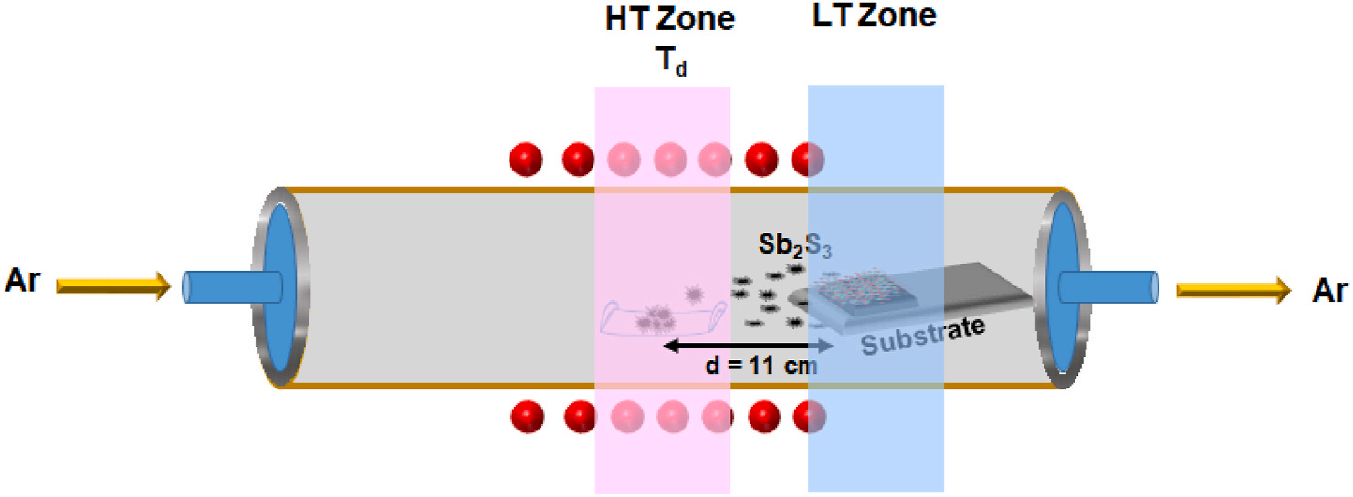
Utilizing a conventional single-zone heating tube furnace (S & R Korea, SRDVF - LV - 3B - 1608), Sb2S3 thin films were deposited using the VTD technique. A quartz tube was incorporated into the single-zone furnace so that the center of the furnace and the quartz tube could sustain a uniform heat distribution within the tube. SLG/Mo (Modeposited soda lime glass) was used as the substrate for deposition. Prior to deposition, a two-step cleaning process was employed. The first step involved 10 min of ultrasonication in IPA, followed by ultrasonication in DI water in the second step. Fig. 1 presents a schematic of the VTD system used for deposition. As-obtained 0.2 g Sb2S3 (99.999%, iTASCO) was used as a precursor and placed at the center of the furnace. The SLG/ Mo substrate was placed on a quartz plate and positioned at a distance of 11 cm from the precursor material within the quartz tube - see Fig. 1. The precursor temperature was tuned from 480 to 540 ◦C using an interval of 20 ℃.

Fig. 1. Schematic of the vapor-transport deposition (VTD) set-up used for Sb2S3 thin-film deposition.
An n-type CdS buffer layer with a thickness of ~60 nm was deposited on the VTD-Sb2S3 thin film absorber layer, followed by CBD. During the CBD process, the three precursor solutions containing 500 mL cadmium sulfate (0.0031 mol/L, CdSO4, ≥99.99%, Sigma-Aldrich), 250 mL ammonium hydroxide (2.87 mol/L, 28.0–30.0%, NH4OH, SigmaAldrich), and thiourea (0.2 mol/L, CH4N2S, ≥99.0%, Sigma-Aldrich), were mixed to obtain 1000 mL at 60 ◦C bath temperature. Here, high concentrations of sulfur resources were used to avoid the Sb oxide–hydroxide formation due to hydrolysis and corrosion. The process was carried out at 500 rpm for 21 min. Furthermore, RF magnetron sputtering was used to deposit a ~70 nm thick window layer of intrinsic ZnO (i-ZnO) followed by a ~ 450 nm thick layer of Al-doped ZnO (AZO) on VTD-Sb2S3/CdS layers (p-n junction). Finally, DC sputtering was used to deposit Al front contacts using the shadow-mask technique. The thickness of the Al contacts was ~1 μm. The mechanical scribing technique produced 0.3 cm2 cell areas in the substrate-configured solar cell devices.
3. Results and discussion
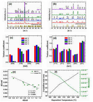
Sb2S3 thin films were layered onto the Mo/SLG substrate via the VTD method at different deposition temperatures, i.e., 480 ◦C, 500 ◦C, 520 ◦C, and 540 ◦C. X-ray diffraction (XRD) was performed on the deposited films to gain insights into the crystalline structure, phase, and orientation of the VTD-Sb2S3 thin films, illustrated in Fig. 2a. The diffraction peaks detected in the XRD pattern reveal the deposition of the orthorhombic stibnite phase of Sb2S3, as indexed by JCPDS no. 42–1393. A comparison of the XRD pattern in Fig. 2a indicates that the dominating (hkl) plane for low deposition temperatures (480 ◦C and 500 ◦C) are a mixture of (120), (130), (211), and (221), whereas (211) and (221) are the dominating (hkl) planes for high depositiontemperatures (520 ◦C, 540 ◦C). Furthermore, the texture coefficient (TChkl) for a designated plane was computed using magnified XRD patterns (Fig. 2b). This was done to assess the preferred orientation of VTD-Sb2S3 on the Mo/SLG substrate, as expressed in Equation (1).

Fig. 2.
4. Conclusion
To summarize, we introduced an adaptable and highly efficient VTD method for depositing Sb2S3 thin films on various substrate configurations of thin-film solar cells (TFSCs). We have observed a significant impact on the crystallinity and, consequently, the performance of the TFSCs when the deposition temperature varied between 480 and 540℃. The characterization of the deposited Sb2S3 thin films, including their crystallinity, surface morphology, and elemental composition, was done using XRD, FE-SEM, and EDS mapping. The XRD results revealed a shift in the crystallite orientation of the films from the (hk0)-plane to the (hk1)-plane when the deposition temperature exceeded 520℃. Furthermore, the surface roughness decreased with increasing deposition temperature, according to the AFM analysis. Notably, the TFSC fabricated using VTD-deposited Sb2S3 thin films at 520℃ exhibited the highest PCE (approximately 0.22%) and VOC and JSC values of 0.511 V and 2.37 mA cm− 2 . The FF remained consistent across all fabricated devices. The present investigation into the effects of deposition temperature on VTD-Sb2S3 TFSC represents a significant step toward harnessing the full potential of this technology. In other words, by optimizing the deposition process, we should be able to pave the way for more efficient and sustainable solar energy solutions. This study not only advances the field of photovoltaics but also charts a course for a more sustainable and eco-friendly future.