ABSTRACT
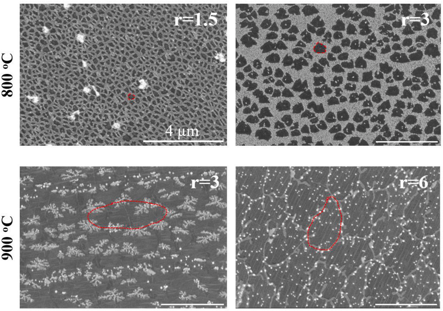
Porous single-layer graphene is promising as the selective layer for membrane-based gas separation thanks to the atomic thickness of the pore which can yield high permselective flux. Direct synthesis of porous graphene by chemical vapor deposition (CVD) is highly attractive to reduce the number of steps in membrane fabrication. This has been demonstrated in the past by incorporating pores as grain-boundary defects, however, pore density in graphene has been limited because of challenges in increasing grain density of single layers to nanocrystalline regime. Herein, we systematically tune the CVD conditions including growth temperature, methane partial pressure and methane/hydrogen ratio to find a low-temperature growth regime where continuous unfragmented graphene film could be synthesized while avoiding multilayers. The resulting graphene is nanocrystalline composed of misoriented nanometer-scale grains with a high density of hydrogen-permeable multivacancy defects or pores. Centimeter-scale single-layer porous graphene membranes yield extremely high H2/SF6 selectivity, reaching above 1000, confirming the high-quality of porous graphene with pores smaller than 0.55 nm, consistent with the structure and distribution of vacancy defects revealed with microscopy.
1. Introduction
Graphene, composed of a single-layer of a two-dimensional array of carbon atoms, is highly attractive for membrane-based gas separation due to its remarkable properties. This includes high mechanical strength for an atom-thick material, high chemical resistance, the flexibility of the film, and the possibility to incorporate carbon vacancy defects to incorporate porosity. Physical etching of graphene lattice, involving high energy radiation exposure to graphene, was one of the first reported methods to incorporate pores on the lattice. Examples include exposure of electron and ion beam to knock out C atoms from the pristine lattice. However, this method could not yield gas-sieving Å-scale pores because of a large difference in energy barrier for knocking out carbon atom from pristine lattice (21 eV) and that from the pore edge (~14 eV) . Instead, oxidation has been shown to yield Å-scale pores successfully. This includes controlled post-synthetic reaction with O2 , O2 plasma, O2 plasma/O3 , and O3 .
Low-temperature CVD has been reported by plasma-enhanced CVD (PECVD) , atmospheric pressure CVD (APCVD) , and low-pressure CVD (LPCVD) . An extremely low synthesis temperature (~350 ◦C) was reported by PECVD due to the faster dissociation of hydrocarbons in the presence of plasma. However, it is challenging to control number of the graphene layers, defect density, and defect size by this method. Energetic ions in plasma can concomitantly damage the surface of graphene which increases the complexity of the method . In APCVD, oxygen and water molecules are challenging to avoid, which greatly influence the synthesis. LPCVD has emerged as an attractive technique to obtain fine control over graphene defects because the concentration of precursors can be finely tuned while avoiding contaminations in the reaction conditions. LPCVD has been demonstrated to synthesize porous single-layer graphene in the temperature range of 800–900 ◦C for gas separation and ion sieving.
2. Experimental methods
Graphene membranes were prepared by transferring graphene from Cu to a commercial porous polymeric support (polyethersulfone (PES), 0.2–0.8 μm-sized pores) using a mechanical-reinforcement strategy. A high-free volume polymer, poly(trimethylsilyl)propyne] or PTMSP, was used as a support film over graphene to ensure high-quality transfer and membrane fabrication, avoiding cracks and tears in graphene. For this, 3 % wt. PTMSP (abcr GmbH) in toluene was spin-coated (1000 rpm for 1 min) on the graphene/Cu surface. The film was dried overnight at room temperature. The resulting PTMSP support film had a ∼ 1 μm thickness. Next a thermal release tape (TRT, Nitto) was laminated on top of PTMSP as additional support. This allowed one to simply lift the sample by a tweezer making the transfer process simple to implement. Subsequently, the Cu foil was etched away using 0.5 M FeCl3 solution, and graphene/PTMSP/TRT was rinsed with 10 wt% HCl solution, and then washed with deionized water. Next, graphene/PTMSP/TRT was placed on the PES support and dried under ambient conditions. In the last step, TRT was removed by heating to 130 ℃ for 2 min. The membrane preparation steps are summarized in Figure S1.

Fig. 1.
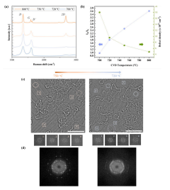
AC-HRTEM images confirmed that defect density increased with decreasing growth temperature (Fig. 2c). The overall defect density was 1.5 ± 0.3 × 1012 cm− 2 at 750 ◦C increasing to 2.5 ± 0.5 × 1012 cm− 2 at 720 ◦C. While this density is lower than that estimated by Raman spectroscopy, we note that in case of Raman, different distortions can activate the D peak in the Raman spectra from Stone-Wales defects and small vacancy defects that are not permeable to gas molecules to large permeable vacancy defects. It is challenging to correctly estimate the density of small defects by AC-HRTEM mainly because of defects attracts contamination which then mask small defects relative easily . Not surprisingly, the degree of contamination increased with the degree of defects (Figs. S9–S11).

Fig. 2
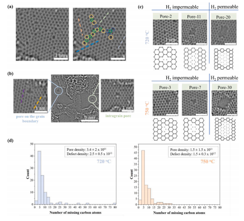
We observed several intragrain defects (Fig. 3b, Fig. S13). Such defects may form due to the trapping of defective state during the crystallization of graphene. At high temperatures, such defects can heal as the crystallization progresses. However, a reduced synthesis temperature can retain these defects on the lattice because of the difference between the energy barrier required for defect formation (1.3 eV) and defect healing (1.86 eV) . Given the temperature-activated nature of these two events, lower synthesis temperature reduces the possibility of defect healing much more than that for defect formation. Therefore, the decrease in temperature increases the number of defects on the graphene lattice.

Fig. 3
4. Conclusions
Overall, we demonstrated a promising direct synthesis approach for porous atom-thick graphene hosting a high density of H2-selective pores. This was possible by a novel synthesis protocol involving reducing the CVD temperature below 800 ◦C and optimizing precursor concentration and precursor/hydrogen ratio. Low temperature growth increased nucleation density of graphene, to an extent that nanocrystalline misoriented grains could be realized, which upon imperfect intergrowth, led to a high density of multivacancy defects, specifically pores larger than pore-13 attractive for sieving hydrogen. To the best of our knowledge, this is the first report of nanocrystalline unfragmented (continuous) single-layer graphene.
The graphene film could be prepared with high-quality, that is the film was continuous over a macroscope without any large pinholes. This was demonstrated by successful sieving of H2 from multivacancy defects. The demonstration of high H2/SF6 selectivity from a centimeterscale graphene membrane is a proof of a uniform growth of the porous graphene film.
We note that 1000 ◦C Cu annealing was required to reduce oxidized domains in the low-cost Cu foil to obtain a continuous graphene film. However, in a continuous roll-to-roll manufacturing, Cu annealing is decoupled from the graphene growth, i.e., Cu annealing can be carried out rapidly in high-temperature setup while graphene growth can be carried out subsequently in a low-temperature setup. The method demonstrated here will help efforts to simply the synthesis of porous graphene, in particular, with the advantage of a reduced energy consumption and lower complexity of the heating setup for graphene CVD.