Abstract: Micro-LED is considered an emerging display technology with significant potential for high resolution, brightness, and energy efficiency in display applications. However, its decreasing pixel size and complex manufacturing process create challenges for its integration with driving units. Recently, researchers have proposed various methods to achieve highly integrated micro-structures with driving unit. Researchers take advantage of the high performance of the transistors to achieve low power consumption, high current gain, and fast response frequency. This paper gives a review of recent studies on the new integration methods of micro-LEDs with different types of transistors, including the integration with BJT, HEMT, TFT, and MOSFET.
1. Introduction
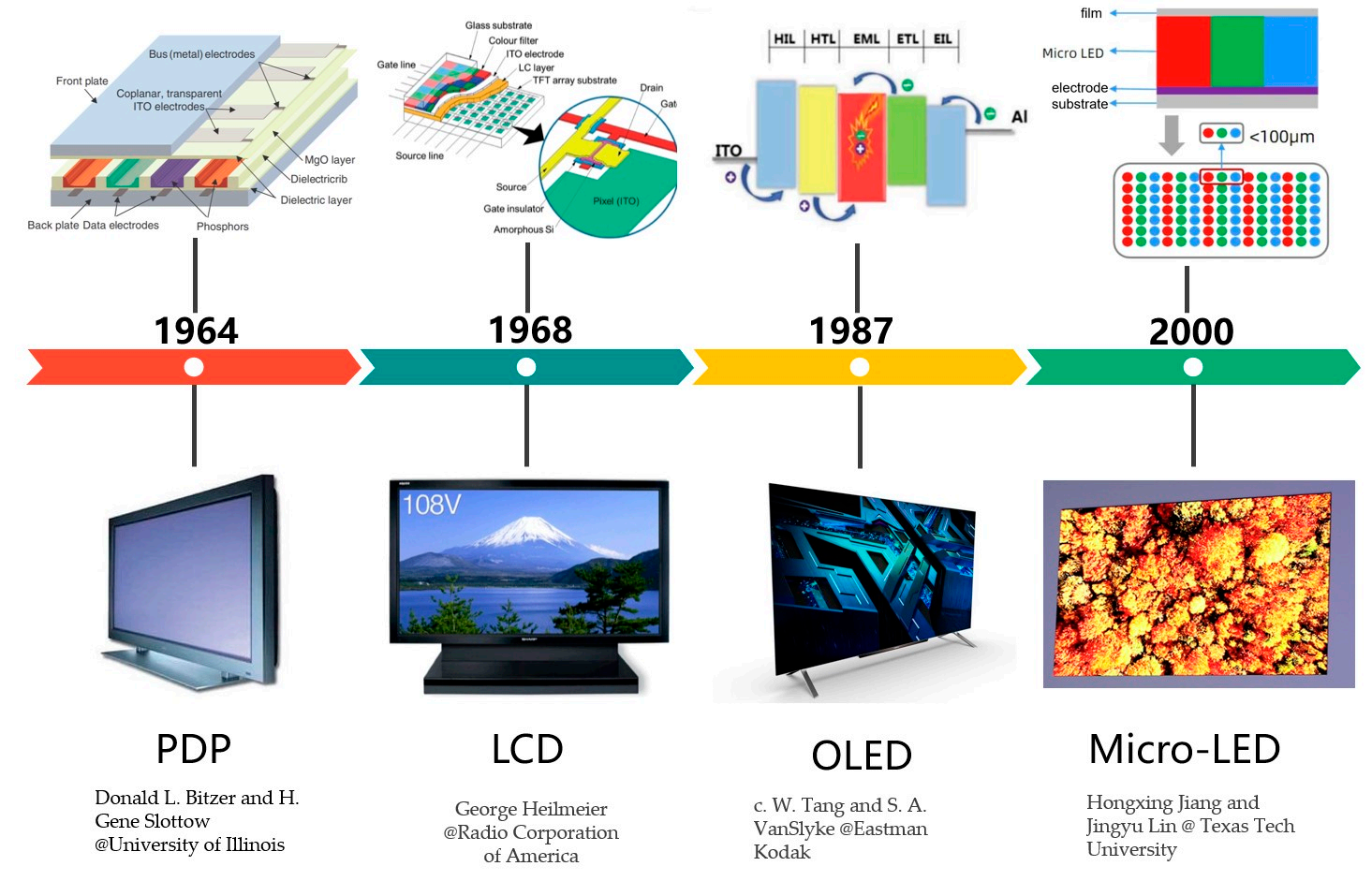
Half a century ago, plasma display (PDP) technology was a popular display technology for time. PDP creates an image by exciting a phosphor to emit light through the discharge of ionized gases. Due to its high energy consumption and high costs, PDP was gradually replaced by other display technologies. Subsequently, liquid crystal display (LCD) monitors, which can regulate the brightness and color of pixels by controlling the arrangement of liquid crystal molecules and the polarization of light to display the image, became popular as the dominant display technology for nearly half a century. Now, organic light-emitting diode (OLED) display technology is an important display technology, which uses the electroluminescence of organic materials to produce images. It does not require a backlight and therefore has a higher contrast ratio, a wider viewing angle, and a faster response time. OLED consists of a stack of organics (ITO) sandwiched between a cathode and anode, where electrons and holes are injected from the electrodes into the organic layer for compounding and light emission. In recent years, the development of OLEDs has centered around two main areas: increasing the optical output power and thinning the device architecture. Currently, researchers are mainly using ordered structures such as (surface mounted) metal–organic framework (SUR) MOFs to regulate electron–hole mobility. This approach can enhance the optical output power while simplifying the structure of OLED devices. They also have great potentials for applications in the field of wearable devices and flexible displays.
In recent years, newly developed micro-LED displays have attracted a lot of attention. A micro-LED is a specially designed LED with an extremely small pixel size, which is capable of achieving high-definition, high-brightess, and high-contrast display perfor.mance [5-10]. The high efficiency ofGaN-based-LEDs could offer low power consumptioncompared to other techniques. Currently, micro-LED displays have demonstrated greatpotential in near-to-eye applications, but they are still facing many challenges in terms ofmanufacturing and integration. Wearable devices, for example, virtual reality (VR) andaugmented reality (AR) devices, high-definition large displays, and other areas, requireextremely high performance from both micro-LEDs and driving units as well. With thecontinuous development and maturity of the micro-LED technique, it is expected thatmicro-LED displays will find a place in the future market and become the next dominantdisplay technology.
Micro-LED technology was firstly proposed by Prf. jiang and Prof. Lin in lexas lechUniversity. Generally, it is widely accepted that micro-LEDs do not exceed 50 microns in sizeFor different display applications, there are two main trends. One of the directions is thatwhich Sony is focusing on, which is small-pitch, high-resolution, large-size indoor/outdoordisplays. The other is the wearable devices (such as AR/VR and Watch) launched by Applewhich require high resolution, portability, low power consumption, and high brightness. Itis important to make the use of the many advantages of micro-LEDs: fast response timehigh brightness, wide viewing angle, high dynamic range, low power consumption, andlong lifetime. The history of display technology is shown in Figure 1.

Figure 1. Development of display techniques.
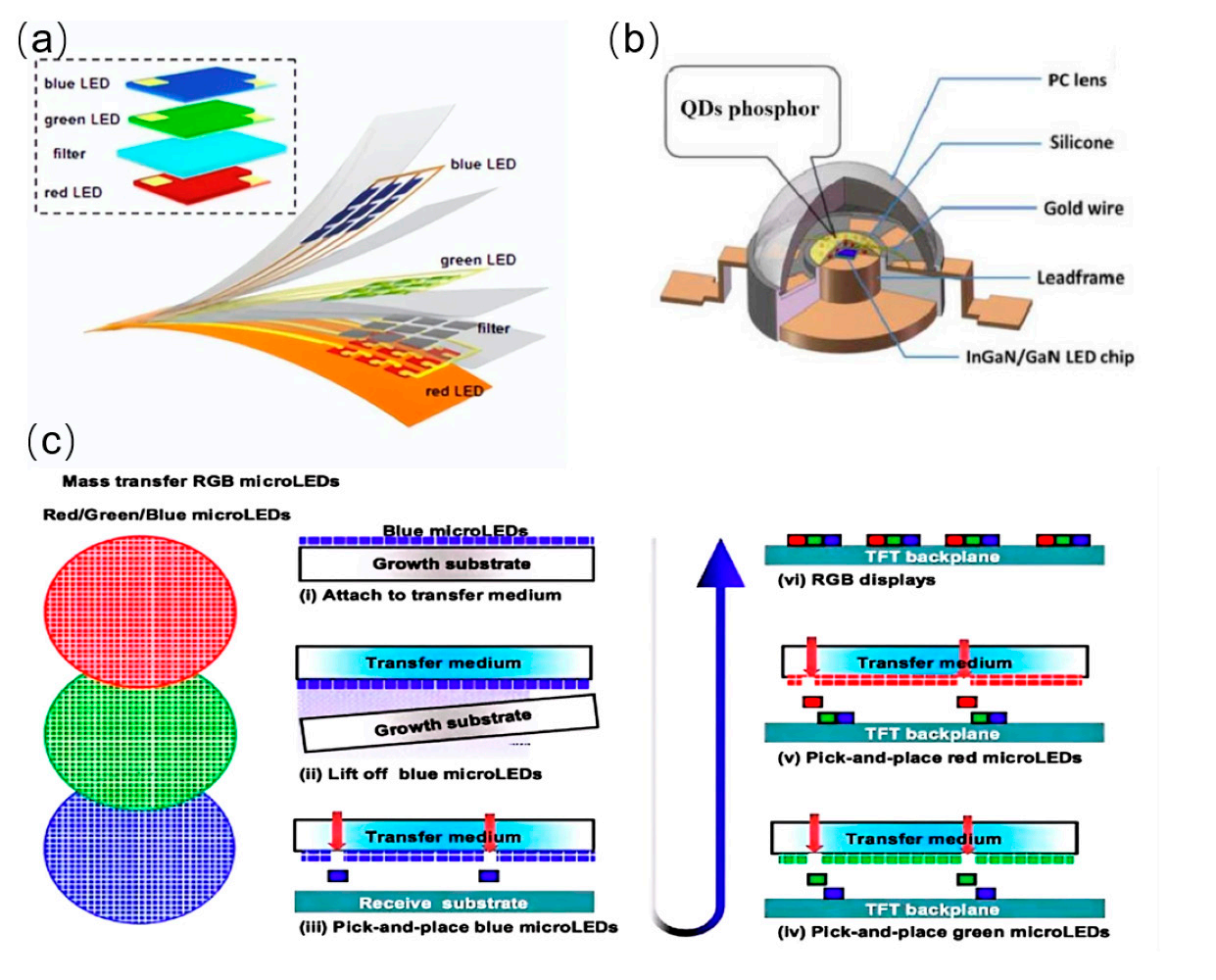
Three-color stacking: The three-color stacking technology achieves the full color display by controlling each vertically stacked red, green, and blue micro-LED, as shown in Figure 2a. The stacking structure allows individual pixels to occupy less space, thereby achieving a higher pixel density per unit area, meeting the requirements for application in small-size micro-display devices and also having wide applications in the display field. Therefore, it is considered to be one of the key technologies for achieving high resolution and high brightness in the future, if it can overcome the difficulty in chip manufacturing and packaging technology. After all, it needs a complex optical design, precise spacing, and accurate alignment of different layers. Color uniformity and consistency, as well as interconnections with driving units, are all challenges that need to be solved for three-color stacking.

Figu re 2. (a) Schematic of three.color stacking technology. (b) $chematic of a light-emitting quantum dot. (c)Schematic of mass transfer.
There are several ways to drive micro-LEDs, the most commonly used being TFT andCMOS driver circuits as shown in Figure 3. The discrete driver allows each micro-LED tobe individually controlled by driver circuits to achieve color, brightness, etc.

Figure 3. Development of micr-LED driver display.
TFT driver circuit: The TFT (Thin-Film Transistor) driver circuit is an active matrix driver circuit commonly used in current displays. It is widely used in various types of flat panel displays, such as LCD TVs, laptop computer displays, mobile phone screens, and so on. The TFT driver circuit usually consists of a driver chip, a TFT array, and power/signal lines. The driver chip is the core part, receiving external signals and controlling the conduction and turn-off of the TFT. The TFT array works as a current switch to control the brightness and color of each pixel by changing the conduction state. The transistors are usually made of monocrystalline or polycrystalline silicon and have high current driving capability and low switching voltage. Power and signal circuits are used to provide power and transmit control signals. Multiple supply voltages and clock signals are usually required to ensure that the thin-film transistors operate properly.
In recent years, amorphous oxide semiconductor materials, represented by IGZO, have received extensive attention for their rich properties. Compared to conventional a-Si TFTs, it has the advantages of good uniformity, simple manufacturing, low manufacturing cost, and high carrier mobility. Besides, IGZO is a wider energy bandgap ~3 eV material with good transparency and has become one of the alternative materials for transparent displays.
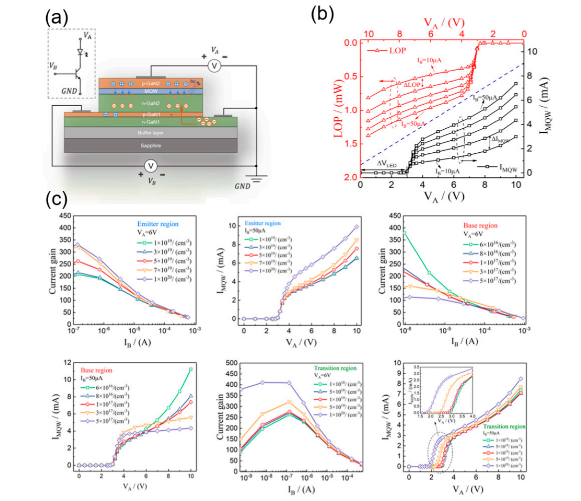
An ideal bipolar transistor (BJT) consists of two pn structures with different doping concentrations. In 2022, S. Hao et al. from Fuzhou University simulated a new type of lightemitting triode, as shown in Figure 4a . One GaN-based LED was vertically integrated with one npn-type BJT on the same chip, where the cathode of the LED and the collector of the BJT share the same n-GaN layer. This vertically integrated structure provides the ability of acquiring higher-resolution display compared to HEMT and MOSFET integration. The optical output power of the integrated device can be regulated by a smaller base-level current. The cut-off frequency can be raised up to 80 MHz and more. The luminous intensity is closely related to the frequency, amplitude, and duty cycle of the pulse signal, proving a stronger capability of controlling the device. However, there are still many difficulties in the process to be solved. The difference in epitaxial temperature and lattice mismatch between P-GaN and N-GaN will result in a poor device performance.

Figure 4. (a) Equ ivalent circuit and operating schematic of the device. (b) Output characteristics andoptical output power characteristics of the device. (e) Current gain and output characteristics fordifferent doping concentrations in the emitter, base, and transition regions.
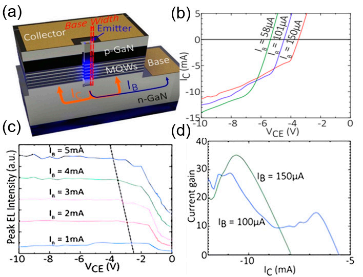
As shown in Figure 5c, the integrated LEB]T with the larger emitter area exhibited alinear relationship between the peak EL, intensity with respect to the base current intensityunder the voltage of Vce = 5 V, demonstrating its electro-optical emitter-like functionReduced emitter area can provide a higher current gain. An average current gain of 20 anda bandwidth of 180 MHz were obtained by nanorods array.

Figure 5. (a) 3D schematic of the device crss-section, (b) I-V characteristic curves of the emissionregion of the nanostructures. (e) EL mapping of the monolithic B]'T structure. (d) Curent gainextracted from the I-V curves.
HEMT-integrated micro-LEDs show good controllability of emission brightness by injecting current, proving their feasibility in a wide range of applications, such as smart watches, HUDs, and AR/VR. GaN-based HEMTs have high-speed switching characteristics and excellent high frequency performance, and thus can provide support for fast current control and regulation, in other words improving the refresh rate of displays. HEMTs have higher current density and power carrying capacity, and can provide higher current drive for LEDs to achieve higher brightness and light output power. Better current spreading can be achieved by optimizing the device structure and material selection. This helps to improve the uniformity and stability of light output. However, the regrowth of HEMTs inevitably brings the problem of thermal and lattice mismatch, increasing the manufacturing costs. We often use enhancement transistors as driving circuits to reduce energy consumption, but it is difficult to fabricate depletion-mode HEMTs.
Overall, the on-chip integration technology of micro-LEDs with driving circuits hasmade significant breakthroughs. In comparison to traditional methods such as mass transferand bonding techniques, the novel approach ofintegrating drivers and displayelementson a single chip demonstrates numerous advantages. The drop in threshold voltage from2.9 to 0.8 V represents a significant reduction in power consumption. The increase in carriermobility from 10.5 to 1810cm'/(V.S) means a faster response frequency. Furthermoremonolithic integration technology not only plays a vital role in the display domain butalso holds immense potential in various other fields, including visible light communicationand chip-level optical interconnection. It is believed that through the efforts of anincreasing number of researchers, the performance of integrated devices will be furtherenhanced, device structures will become more streamlined, and functionalities will grow.more diverse. In the near future, on-chip integration technology is proposed to have broader application prospects within the realm of micro-LED displays