Abstract:This manuscript provides an introduction to third-generation semiconductor material, singlecrystal silicon carbide (SiC), offering a concise overview of its fabrication process. It delves into the chemical mechanical polishing of SiC wafers employing silica (SiO2) and ceria (CeO2) abrasives; it examines the variations in the wettability of SiC surfaces with pH changes, noting reduced contact angles and increased spreading coefficients in highly acidic and alkaline conditions. The study further analyzes the impact of SiO2 abrasive concentration, revealing that an increase to 8wt% leads to a peak material removal rate of 185 nm/h. Predictive forces based on DLVO theory suggest that SiO2 particles are prone to adhesion on the wafer surface within the pH range of 2-5, primarily due to DLVO-induced electrostatic attraction, which can result in surface contamination. In contrast, adsorption theories predict that CeO2 particles are likely to adhere to the wafer surface in both acidic and alkaline solutions, predominantly through the chemical chelating actions of CeO2 particles, without contaminating the surface.
1. Introduction
In recent years, semiconductor materials have risen to prominence as a burgeoning industry, playing an increasingly pivotal role in cutting-edge technologies and the national economy. Exemplified by gallium nitride (GaN) and silicon carbide (SiC), third-generation semiconductors exhibit superior characteristics such as high-temperature resistance, high-voltage tolerance, high-frequency operation, high power capabilities, and radiation hardness. Despite these attributes, their application has been historically constrained to a limited scope due to factors such as manufacturing processes and costs. However, with continuous breakthroughs in material growth and device fabrication techniques, the costperformance ratio of third-generation semiconductors is gradually becoming apparent, thereby catalyzing their penetration into the market. SiC components have been employed in automotive inverters, while GaN-based fast chargers have been widely commercialized. Over the next five years, electronic devices founded upon third-generation semiconductor materials are anticipated to find extensive applications across various domains, including 5G base stations, renewable energy vehicles, ultra-high voltage systems, and data centers.
Silicon carbide (SiC), as the quintessential representative of third-generation wide-bandgap semiconductor materials, significantly outperforms first-generation elemental semiconductors (Si) and second-generation compound semiconductors (GaAs, InP, etc.) in both performance and reliability. This is particularly true in extreme conditions and harsh environments, making it an asset with vast potential for deployment in the realm of high-performance power semiconductor technology. Nonetheless, the inherent hardness, brittleness, and chemical inertness of SiC present substantial challenges in achieving wafer thinning and ensuring damage-free, smooth surfaces. On one hand lies the material’s intrinsic processing difficulty; on the other, the stringent substrate specifications for epitaxial layers in integrated circuit fabrication demand flawlessly flat and ultrasmooth surfaces, virtually free from defects or damage. In concert with the advances propelled by smart technologies and the Internet of Things, the functionality and applications of integrated circuit chips have expanded, necessitating that substrate wafers evolve towards diminished thickness and enhanced, ultra-smooth, undamaged surfaces to accommodate the sophisticated requirements of high-end chips.
In contrast to conventional mechanical polishing, the Chemical Mechanical Polishing (CMP) process of SiC wafer introduces a chemical effect. The chemically induced oxidation by oxidizers within the polishing slurry leads to the formation of a softened SiO2 layer on the surface of the SiC wafer through the transformation of SiC into SiO2. This enhances the machinability of the SiC wafer's surface. Subsequent mechanical abrasion by the abrasive particles removes this softened layer, thereby facilitating the elimination of material from the SiC wafer's surface and yielding a superior polished finish, as depicted in Figure 1. Consequently, the generation of the surface oxidized softening layer is central to the CMP process of SiC wafers, representing a pivotal step that determines the material removal rate. Chemical Mechanical Polishing (CMP) stands as one of the most efficacious methodologies to attain an ultra-smooth and damage-free SiC wafer surface.
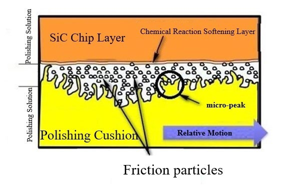
Figure 1: Chemical mechanical polishing mechanism illustration
To address the limitations of traditional mechanical polishing, contemporary advancements have led to the development of Chemical Mechanical Polishing (CMP). This process synergistically combines chemical etching and mechanical abrasion to remove and flatten surface materials on workpieces. During polishing, the wafers undergo chemical oxidation in the presence of the polishing slurry, leading to the formation of a chemically reactive layer. Subsequently, this softened reactive layer is removed under the mechanical action of the abrasives. The Chemical Mechanical Polishing apparatus is illustrated in Figure 2. This report primarily investigates the DLVO theory and adsorption mechanisms during the Chemical Mechanical Polishing of SiC wafers using SiO2 and CeO2 abrasives.
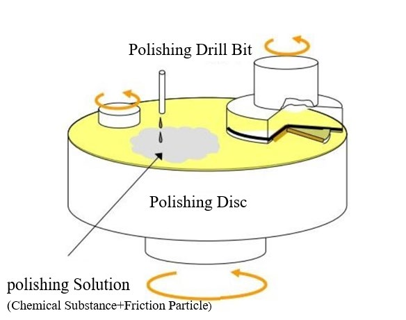
Figure 2: Chemical mechanical planarization apparatus diagram
2. The wettability analysis of polishing slurries on 6H-SiC wafers
Figure 3 presents a schematic representation of the interfacial free energy when an aqueous solution is placed upon the surface of a 6H-SiC crystal sample, where θ denotes the contact angle at the threephase boundary.
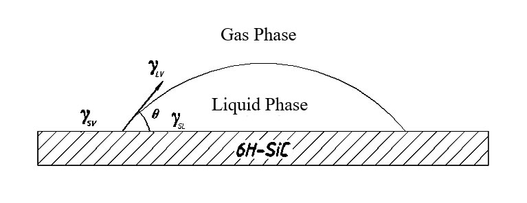
Figure 3: Diagram illustrating the surface interfacial free energy of 6H-SiC wafers
Investigators ascertained the profile of the contact angle θ as a function of pH in aqueous solutions as delineated in Figure 4. It is evident from the figure that the contact angle initially escalates with an increase in pH, attaining a zenith between pH 5 and 6[3], before subsequently diminishing. A diminished contact angle characterizes both the low and high pH extremities on the chip surface. A quintic polynomial regression applied to the data in Figure 4 yielded a correlation coefficient, R2 , of 0.99. The regression revealed a maximum contact angle of 58.0°, corresponding to a solution pH of approximately 5.5. The apex of the three-phase contact angle indicates the minimization of electrostatic interactions at the solid-liquid interface, designating this particular pH as the point of zero charge for the interface.
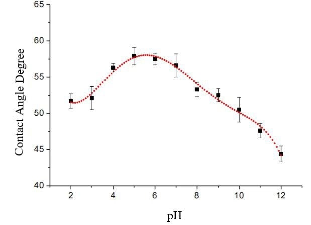
Figure 4: The variation curve of the contact angle as a function of pH
3. The role of SiO2 abrasives in the polishing process of 6H-SiC wafers
Abrasive particles play a pivotal role in the mechanical removal during the CMP polishing process, representing a critical component within the polishing slurry. Their hardness, size, concentration, morphology, and properties considerably influence the efficiency of polishing. Researchers have investigated the impact of slurry pH and abrasive concentration on the CMP outcomes of 6H-SiC wafers using colloidal SiO2 as the abrasive medium through experimental studies.
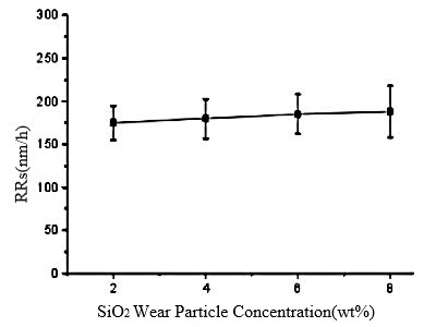
Figure 5: The concentration of SiO2 abrasives significantly influences the polishing outcome
As the concentration of SiO2 abrasives increased from 2wt% to 6wt%, the material removal rate escalated from 175 nm/h to 185 nm/h. However, further augmentation of the SiO2 concentration to 8wt% did not alter the removal rate significantly, as illustrated in Figure 5. The primary function of SiO2 particles during the CMP polishing of 6H-SiC wafers is mechanical abrasion. With the increment in silica concentration, the mechanical action intensifies during polishing, thereby increasing the material removal rate. Nevertheless, as the concentration of SiO2 particles continues to rise from 6wt% to 8wt%, the contact area between SiO2 abrasives and the surface of the 6H-SiC wafer reaches its maximum, resulting in a saturation of mechanical effects and thus, the material removal rate remains essentially unchanged.
4. Conclusions
In summary, the DLVO theory-based predictions of adhesive forces indicate that SiO2 particles are prone to adhere to wafer surfaces within the pH range of 2 to 5. This adhesion, primarily driven by DLVO electrostatic attraction, results in the SiO2 particles being adsorbed onto the wafer surfaces through electrostatic interactions, inhibiting the oxidative hydrolysis of the surface, reducing the material removal rate, and contributing to particulate contamination of polished surfaces. Conversely, predictive forces based on adsorption theories suggest that CeO2 particles readily adhere to wafer surfaces in both acidic and alkaline solutions, predominantly due to the chemisorptive interactions of the CeO2 particles. The adherence of CeO2 particles, facilitated by chemical bonding, not only does not obstruct the oxidative hydrolysis of wafer surfaces but also promotes the removal of oxidized material without causing particulate contamination of the polished surfaces.
下一篇: 铌薄膜结构对超导电路损耗的影响