The performance of superconducting microwave circuits is strongly influenced by the material properties of the superconducting film and substrate. While progress has been made in understanding the importance of surface preparation and the effect of surface oxides, the complex effect of superconductor film structure on microwave losses is not yet fully understood. In this study, we investigate the microwave properties of niobium resonators with different crystalline properties and related surface topographies. We analyze a series of magnetron sputtered films in which the Nb crystal orientation and surface topography are changed by varying the substrate temperatures between room temperature and 975 K. The lowest-loss resonators that we measure have quality factors of over 106 at single-photon powers, among the best ever recorded using the Nb on sapphire platform. We observe the highest quality factors in films grown at an intermediate temperature regime of the growth series (550 K) where the films display both preferential ordering of the crystal domains and low surface roughness. Furthermore, we analyze the temperature-dependent behavior of our resonators to learn about how the quasiparticle density in the Nb film is affected by the niobium crystal structure and the presence of grain boundaries. Our results stress the connection between the crystal structure of superconducting films and the loss mechanisms suffered by the resonators and demonstrate that even a moderate change in temperature during thin film deposition can significantly affect the resulting quality factors.
I. INTRODUCTION
The effort to build large-scale quantum processors has emphasized how studying materials can improve the lifetime and coherence of quantum systems. Superconducting microwave resonators are often used to investigate loss in superconducting qubits because they are generally simpler to fabricate and measure while all sources of relaxation and decoherence affecting the performance of a resonator will also impact the performance of a qubit made from the same material. Additionally, there are other applications that benefit from superconducting resonators with low levels of microwave dissipation, such as parametric amplifiers, quantum sensors, and microwave kinetic inductance detectors (MKIDs) used for astronomy and particle physics.
TLS. Many investigations attempting to reduce TLS loss have focused on the removal of unwanted oxides and impurities from different interfaces through etching or cleaning steps. Pre-deposition cleaning steps of the substrate to avoid metal-substrate interface losses , as well as post-deposition processing steps of both substrate and deposited metal to reduce losses at the exposed surfaces have been investigated intensively. However, the connection between the superconductor film structure, which is determined by the deposition process, and the microwave loss suffered by circuits is not as well understood. Differences in the deposition process have been previously studied by some authors who also report changes in microwave properties, but an accurate description of the effect of film crystal properties on TLS loss as well as other loss mechanisms has not yet been established.
Our study focuses on niobium, commonly used in the superconducting circuits community because it has the highest critical temperature and critical magnetic field of any elemental superconductor. Furthermore, mono-crystalline Nb growth is possible at sufficiently high temperature and optimised growth conditions. Sapphire substrates offer good thermal as well as chemical stability and have a small lattice mismatch with the Nb lattice, which allows for epitaxial growth. These key properties make Nb on sapphire suitable material platform to study the effect of crystallinity changes on superconducting resonator performance.
II. EXPERIMENTAL DESIGN
For this study, five thin film depositions were performed at various temperatures while all of the other deposition conditions were kept the same. The Nb thin films were sputtered in an Ultra High Vacuum (UHV) deposition chamber using DC magnetron sputtering. The base pressure of the sputtering chamber was below 2 × 10⁻¹⁰ mBar, indicating a low impurity background. The pressure during the deposition was 8.8×10⁻³ mBar and the distance between the 2 inch Nb target and the substrate was 110 mm. The power applied was 125 W corresponding to a stable growth rate of 0.27 nm/s at room temperature determined from in-situ Quartz Crystal Microbalance measurements. The effective growth rate decreased linearly with increasing temperature due to partial re-evaporation of adatoms from the surface. After growth, the thickness was recalibrated using profilometry and Transmission Electron Microscopy (TEM) measurements and the growth time was adjusted to achieve a thickness of around 185 nm for all films. The substrate temperature shown in Tab. I was set based on pyrometer readings of the temperature of the middle of the wafer.
III. RESULTS
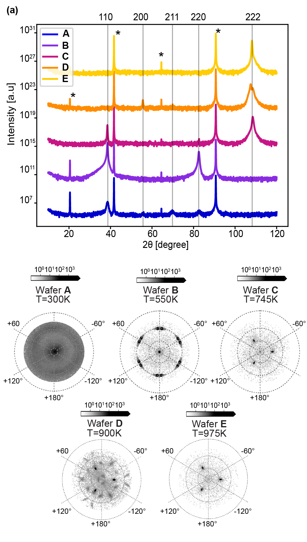
Fig. 1 (a) shows X-Ray diffraction (XRD) traces of the Nb films listed in Tab. I. Various Nb diffraction lines are indicated in the figure. Film A that was deposited at room temperature shows signatures of all the commonly observed diffraction lines of poly-crystalline Nb, namely 110, 200, 211, and 220.

FIG. 1. (a) XRD radial scans of the wafers listed in Table I. The traces are offset with respect to each other for clarity. The sharp peaks that are associated with the mono-crystalline sapphire substrate are labeled with a star. (b) XRD polefigures of the 110 Bragg peak showing the orientation distribution of the direction for films deposited at various temperatures.
The deposition temperature also influences the surface roughness of the sputtered Nb film. The surface topography was measured using atomic force microscopy (AFM) for each individual wafer directly after growth and is shown in Fig. 2 (a). The surface of the wafer grown at room temperature clearly consists of small grains with no apparent preferential orientation. This grain structure of Nb has been frequently observed on a large variety of substrates such as Si and GaAs. A distinct triangular pattern appears at 550 K that becomes more and more evident with increasing temperature. The schematic in Fig. 2 (c) illustrates how a top view of the Nb (111) lattice planes could result in the observed triangular geometry. Our data suggests that the crystal domains grow in size and consequently change the surface roughness and morphology in a complex process of self-assembly during growth. The effect on the rootmean-square (RMS) surface roughness calculated from the 2×2 µm AFM areas is plotted in Fig. 2 (b). It is evident from this plot that Wafer B has the lowest surface roughness.
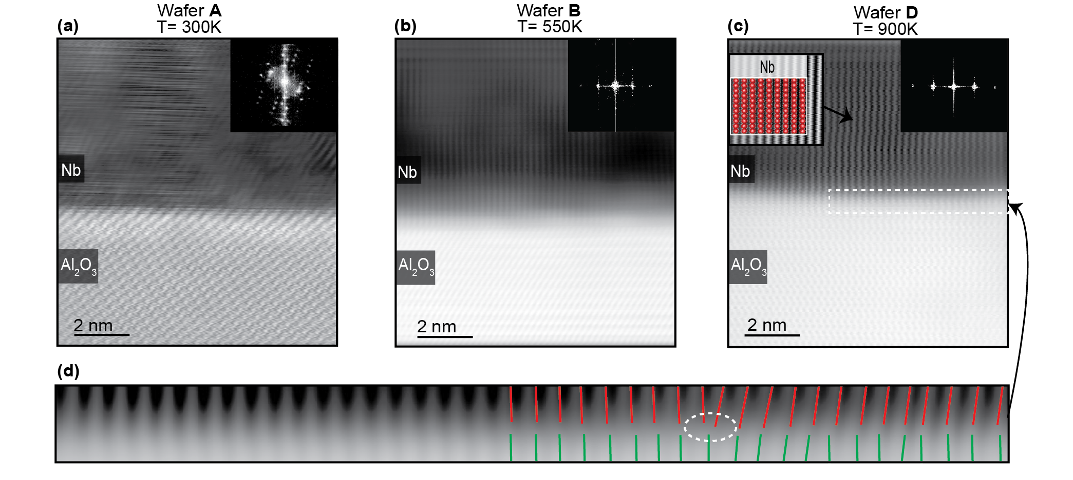
Another key feature that is known to have an effect on superconducting microwave resonator performance is the quality of the interface between the superconductor and the substrate. We investigated the Al2O3-Nb interface of Wafers A, B and D using Scanning Transmission Electron Microscopy (STEM). In Fig. 3 (a), it can be observed that for films grown at room temperature, a high-quality non-epitaxial interface is obtained that does not show any signs of oxides or chemical intermixing. The poly-crystalline character of the Nb layer is further substantiated by the ring-shaped pattern observed in the fast Fourier transform (FFT) image in the top right corner. At intermediate growth temperatures, it can be seen in Fig. 3 (b) that an interface with a high degree of epitaxy between the sapphire (0001) and the Nb (110) crystals forms. Some variation in grain alignment was observed on the length scale of the lamella window ((1.5 µm) for Wafer B. In Fig. 3 (c), the Nb to sapphire interface of Wafer D is shown. For this wafer, no grain boundaries were observed on the length scale of the lamella window and the Nb (111) to sapphire interface seems fully epitaxial. Therefore, we conclude that the (200) peak observed in the XRD measurements shown in Fig. 1 is only a very minor portion of the total crystal structure. A crystallographic model of the Nb lattice made using crystal visualization software (VESTA ) is overlaid with a zoomed-in part of the figure and shows agreement with the image. The intense highly symmetrical features of the FFT in the in-set of Fig. 3 (c) clearly confirm the single crystalline nature and high degree of epitaxy in the measured portion of the film. The strain relaxation by the formation of a periodic array of misfit dislocation can be deduced from the Bragg filtered image of Wafer D shown in Fig. 3 (c).

FIG. 3
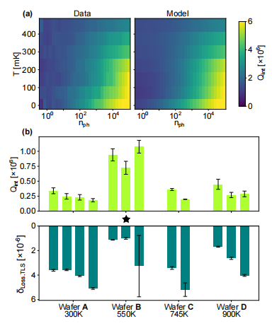
Fig. 4 (a) compares a measurement of the internal quality factor of one resonator from Wafer B to Eq. 1. The excellent agreement indicates that our model captures the temperature and power dependence of the measured quality factors (see Appendix F for the same comparison for all resonators shown in Fig. 4 (b) ). As predicted by TLS theory, the internal quality factor is highest at high power and has a non-straightforward temperature dependence originating from the competition of TLS saturation and TLS interactions. Additionally, fitting to our model allows us to distinguish TLS loss from PI loss. In Fig. 4 (b) we show the low-temperature single-photon quality factors for each resonator that we measured together with the extracted TLS losses. We excluded any resonators with visible fabrication defects. The yield of working resonators varied for each chip but was always ≥ 50%. Resonators from Wafer B, grown at 550 K, show substantially higher quality factors and lower TLS losses than resonators grown at the other temperatures. The highest single-photon Qint we measured was 1.1±0.1×10⁶ , which to our knowledge is among the highest ever measured single-photon Qint for a niobium on sapphire resonator.

FIG. 4.
V. CONCLUSION
In the first section of our study, we show that the crystallographic structure of Nb on sapphire films is drastically affected by changing the deposition temperature.
This resulted in films ranging from a poly-crystalline structure (Sample A) at room temperature to a completely mono-crystalline character at the highest temperature of 975 K (Sample E). With increasing temperature, the films have fewer grain boundaries and the crystal domains undergo an increasing degree of ordering in the preferred orientation. These differences in crystallinity also lead to variation in surface roughness, most notably in Wafer B, which has the lowest surface roughness.
These differences in material properties lead to significant variations in the microwave behavior of our superconducting resonators. Specifically, we found the best single-photon quality factors of over one million in the resonators made from Wafer B, which was grown at an intermediate temperature of 550 K. These quality factors are state-of-the-art for Nb on sapphire resonators, and are within an order of magnitude of the state-ofthe-art for niobium resonators on any substrate . We believe that the TLS loss rate could be further reduced by optimizing the fabrication process by including steps like a HF etch to remove the processing oxide, etching trenches, encapsulating the resonator, or optimizing the CPW geometry for low electric field participation at material interfaces. Our results could also be strengthened by measuring more resonators on more samples, as the TLS losses we report vary from resonator to resonator.