ABSTRACT
Gallium nitride (GaN) integrated circuits (ICs) are receiving increasing attention because they offer compactness, reduced parasitics, and higher performance compared to discrete transistors or printed circuit board (PCB) integration. The p-GaN platform exhibits tremendous potential in power ICs and recently, in high temperature (500 °C) digital circuits. While the initial demonstrations offer promising results, several challenges remain. Notably, the lack of a monolithically integrated GaN complementary technology impedes the advancement of GaN power ICs.
This thesis aims to enhance the p-GaN platform (GaN-CMOS platform) (CMOS: complementary metal-oxide-semiconductor) through developing the next generation of GaN complementary technology (p-channel and n-channel field-effect transistors (FETs)). Based on the GaN-CMOS platform, the aggressive scaling of novel complementary transistors (self-aligned-gate p-FET and self-aligned metal/p-GaN-gate HEMT) is pursued. Alternative metallization schemes and a new technology for gate recess in GaN p-FETs are demonstrated. The unique characteristics of the p-FET are revealed through a combination of experimental measurements and TCAD simulations. The p-FET (based on GaN-CMOS platform) and p-GaN-gate n-FETs are analyzed for high temperature operation. Lastly, in order to aid the future design of more complex circuits based on the p-GaN platform, a device-to-circuit CAD framework was developed for GaN n-FET circuits and validated at high temperature up to 500 °C.
Introduction
With the prevalence of electronics in our daily lives and its increasing role in our smart society, the demand for high performance, energy-efficient, compact electronics has seen an exponential increase. While traditionally microelectronics chips have been used for computation, there has been increasing needs for radio frequency (RF) and power electronics for emerging applications such as electric vehicles, 5G/6G telecommunication, and data centers. Among the various semiconductor technologies, gallium nitride (GaN) stands out as an excellent candidate for both RF and power applications, thanks to its wide band gap, high electron mobility, high breakdown field, thermal and chemical stability and more. Since the advent of the first AlGaN/GaN high electron mobility transistor (HEMT) (then called heterostructure field-effect transistor) in 1993, phenomenal advancement has been made the in the field of GaN electronics.
In the RF-GaN domain, GaN HEMTs are dominant in the RF power amplifiers in base stations (because only this technology is capable of delivering high power with high power-added efficiency (PAE) at microwave and mm-wave frequencies). Extensive research and development (R&D) efforts are under way to introduce GaN HEMTs for lower voltage applications in the RF front-end of cellular handsets, an application area traditionally dominated by Si LDMOS (laterally-diffused metal-oxide semiconductor) and GaAs pHEMTs (p: pseudomorphic).
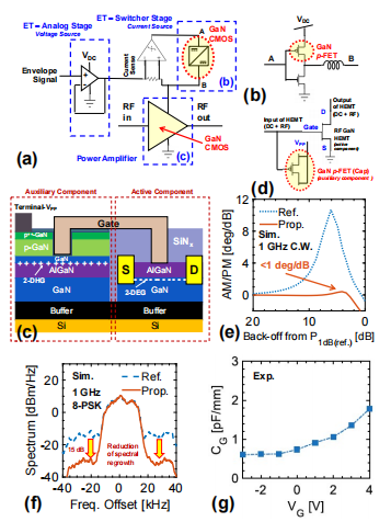
GaN-CMOS technology, if successful, would be a fundamental device-level advancement that could bring about advancements in the RF front end. A simplified schematic of the RF transmitter, consisting of the power amplifier, is illustrated in Fig. 1.1(a). Specifically, two areas are discussed:
GaN CMOS DC-DC converter for use in hybrid ET: The use of a GaN p-FET switch is proposed for a wide bandwidth dynamic power supply to be used in 5G PAs (Fig. 1.1(a)). In the switcher stage (Fig. 1.1(b)), the GaN p-FET would be gated by pulses from the analog stage. Here, no level shifters are required because the high-side switching is performed by the p-FET. Therefore, assuming p-FETs with high switching performance are deployed, GaNCMOS technology is expected to realize wide bandwidth envelope trackers in the power management ICs.

Figure 1.1: Applications of GaN-CMOS technology in the RF front end. (a) Schematic of the RF transmitter. The proposed novel components based on GaN-CMOS technology are highlighted. (b) Circuit diagram of the proposed DC-DC converter used in the switcher stage of the ET. (c) Proposed integrated GaN-CMOS device to achieve higher linearity. (d) Simplified circuit model of the proposed linearized device used in the simulations. Proof-of-concept simulations indicate promising performance: (e) One-tone load-pull at 1 GHz, showing significant reduction in AM/PM to < 1.5 deg/dB. (f) 1 GHz 8-PSK operation, showing reduction in spectral regrowth. Significant improvement in EVM (by > 60 %) at higher receiving channel powers was observed. (g) Preliminary experimental results of a linearized capacitance profile of a GaN n-FET with Vth = 2 V and ON-OFF ratio of 108 .
As a disclaimer, here (and throughout the thesis), the term “GaN-CMOS” refers to the concept of complementary GaN-based transistors (GaN-based p-FET and GaN-based n-FET), similar to the Si-CMOS technology (Si-PMOS and Si-NMOS FETs) prevalent today. The concept may be further extended to complementary transistors based on other III-N materials. In the case of specific transistor structures, the term “complementary transistors” or “complementary technology” (CT) will be used instead, because “CMOS” contains references to the MOS (metal-oxidesemiconductor) structure. “GaN-CMOS” does not typically require a carrier inversion layer as is the case in more conventional Si-CMOS. In this thesis, unless otherwise stated, “complementary transistors” does not refer to the novel device architecture “complementary transistor (CFET)” proposed for Si advanced logic nodes, though GaN-CFET would be a promising area for future work.
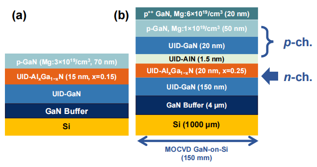
Before introducing the GaN-CMOS platform, it is insightful to review the conventional p-GaN platform, typically used for power HEMTs. A typical epitaxy is shown in Fig. 1.2(a). At the top of the conventional AlGaN/GaN epitaxy (used for E-mode HEMTs), a p-GaN layer is added to ensure normally-off operation, by depleting the 2DEG channel (AlGaN/GaN interface) at zero bias conditions.

Figure 1.2: GaN-CMOS platform. (a) A conventional epitaxy for p-GaN-gate power HEMT, for illustrative purpose. (b) Epitaxial structure of the GaN-CMOS platform used in this thesis. Note that all doping levels are nominal values provided by the supplier. Actual doping profile is affected by non-idealities such as the Mg doping delay and memory effect.
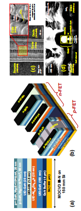
The starting material is the GaN-CMOS platform as shown in Fig. 1.2(b). The epitaxial structure (“Epi-1”, Fig. 2.1(a)) is modified from earlier work by inserting a 1.5 nm AlN (in actual implementation, high Al composition AlGaN) layer. The use of an AlN layer allows for polarization enhancement of the p-channel charge density and a better etch stop during the selective etch of p-GaN/UID-GaN over AlGaN (a key process step for the n-FET). Both p-FETs and n-FETs were fabricated on this structure (Fig. 2.1(b)–(d)). The same epitaxial structure of Fig. 2.1(a) was processed to realize the p-FET and n-FET (Fig. 2.1(b)). In this chapter, unless otherwise stated, the p-FET and n-FET refers to GaN-based transistors.

Figure 2.1: Highly-scaled GaN complementary technology (CT). (a) Epitaxial structure. (b) Device structures of p-FET (SA FinFET) and n-FET (SA-gate p-GaN-gate HEMT) based on the same GaN-on-Si platform as illustrated in Fig. 2.1(a). (c), (d) Scanning electron microscopy (SEM) images of representative p-FET and n-FET, respectively.
Advanced scaling based on self-aligned features, as proposed in this work, offers a viable technology path for future high performance GaN complementary technology based on a MOCVD GaN-on-Si platform. The scaled p-FETs and n-FETs achieve competitive performance in their respective categories, and when taken together, deliver a leading GaN CT solution. An ICP-RIE selective etch was developed with excellent n-FET ohmic contacts obtained. This selective etch could be used in the future GaN-CMOS platform.
Further design innovation and engineering of the proposed technology would greatly benefit the eventual wafer-level heterogeneous integration of GaN CT (based on a Si substrate) with Si CMOS to achieve multi-functional chips.