ABSTRACT
This work demonstrates the potential use of Cu-Sn-In metallurgy for wafer-level low-temperature solid-liquid interdiffusion (LT-SLID) bonding process for microelectromechanical system (MEMS) packaging. Test structures containing seal-ring shaped SLID bonds were employed to bond silicon and glass wafers at temperatures as low as 170 ℃. Scanning acoustic microscopy (SAM) was utilized to inspect the quality of as-bonded wafers. The package hermeticity was characterized by cap-deflection measurements and evaluated through finite element modelling. The results indicate the bonds are hermetic, but residual stresses limit the quantitative analysis of the hermeticity. The microstructural studies confirm the bonds contain a single-phase intermetallic Cu6(Sn,In)5 that remains thermally stable up to 500℃. This work shows Cu-Sn-In based low-temperature bonding method as a viable packaging option for optical MEMS or other temperature-sensitive components.
1. Introduction
Wafer-level bonding is a cost-effective technology for microelectromechanical system (MEMS) packaging. The process enables components to be protected at the early manufacturing stage, which leads to an increase in production yield. The main criterion of effective packaging is ensuring a hermetically sealed environment to maintain optimal device operation. However, optical MEMS also requires the package to have a sensing “window”, which limits the choices of material.
The operating conditions of optical MEMS devices, such as microbolometers and micromirrors, require the cap to have good transparency for light to pass through while maintaining a hermetic environment. Thus, glass-based materials are often selected for their wide transparency window and low gas permeability. Nonetheless, hermetic silicon-to-glass bonding process remains a challenging topic, mainly due to the thermomechanical stresses from high processing temperatures.
Solid-liquid interdiffusion (SLID) represents a promising option for silicon-to-glass bonding. Compared to other bonding methods, the SLID process benefits from low-to-moderate processing temperatures and does not demand strict surface conditions. The resulting bonds have a higher remelting temperature than the processing temperature, low gas permeability, and adequate mechanical strength. Furthermore, the bonds are electrically conductive, which means they can be utilized with through silicon or glass vias (TSVs/TGVs) to form vertical interconnects in heterogeneous integration.
2. Experimental method
2.1. Test vehicle fabrication and characterization
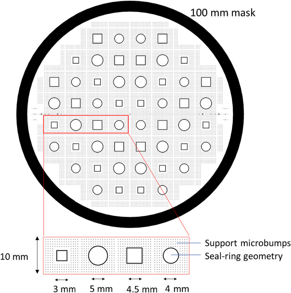
The details of the wafers and bonding temperatures used in this study are listed in Table 1. Borofloat®33 is a borosilicate glass with excellent transmissivity, good thermal resistance, and chemical durability, which make it suitable for micro- and optoelectronics packaging applications. The fabrication procedures were based on the processes presented in . First, the backsides of the silicon wafers were patterned for dicing marks with lithography process followed by reactive ion etching. In preparation for the bonding process, 30 nm of TiW adhesion layer and 120 nm Cu seed layers were sputter deposited on the front side. Then, seal-ring type features were patterned using lithography process. Two types of seal-rings with different shapes and sizes were distributed over the wafer into 52 pieces of 10 mm × 10 mm chips, as illustrated in Fig. 1. Square support bumps with a width of 50 μm were also distributed surrounding the sealing ring to provide structural integrity. Cu-Sn-In metal stacks for the bonding process were then deposited by electroplating process with a thickness of 3.5 ± 0.2 μm, 1.8 ± 0.1 μm, and 2.3 ± 0.4 μm, respectively. Prior to the bonding process, the photoresist was stripped, and TiW/Cu seed layers were removed.

Fig. 1. Masks design for the test vehicle containing four types of sealring geometries.
The wafers were then diced, and the deflection was remeasured using contact and optical profilometer. Some of the chips were then crosssectioned for microstructural observation utilizing scanning electron microscopy (SEM) equipped with energy-dispersive spectroscopy (EDS), focus ion beam (FIB) and electron backscatter diffraction (EBSD). The bonds' mechanical strength was inspected through tensile tests. Shear strength test was not conducted to mitigate the effects of different failure modes coming from microbumps and seal-ring structure. Additionally, the melted metal could form a squeeze-out at the bond edge which also affects the accuracy of shear stress measurement. The tensile test set-up was designed according to the standard Mil-STD-883 K Method 2027.2 for estimating substrate attach strength, as closely as possible [29]. Ten chips from each sample type containing a 3 mm × 3 mm sized squareshaped seal-ring were mounted in copper brass studs. The studs were then installed into the mechanical tensile tester and a strain rate of 0.1.
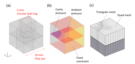
In this work, two case studies were conducted to evaluate the cap deflection. The first one is cap deflection estimation without considering residual stress, while the second study implements residual stresses. The boundary conditions for the first study were as follows: First, a symmetry function was applied to the two quadrant cross-sections. Then atmospheric pressure of 1.01 × 10⁵ Pa was applied to the cap substrate, while the cavity internal pressure was varied between 0.1 and 1.01 × 10⁵ Pa, which refers to the cavity vacuum condition. Fixed constraints were applied to the sidewalls of the substrate since the modelled chip were assumed to be constrained by the neighbouring chips in the wafers. The 3D model in Fig. 2(b) illustrates the area where these boundary conditions were applied. For the second study, similar boundary conditions were applied to the geometry. Additionally, residual stresses were incorporated by adding a thermal expansion node to the model based on the work presented in . To model the cooling down process, the initial temperature was set to the bonding temperature, while the final temperature was set to room temperature of 20 ◦C. Furthermore, the copper layer was assumed to be under plastic loading with an initial yield stress of 250 MPa and isotropic tangent modulus of 2 GPa.
3. Results and discussions
3.1. Hermeticity investigation
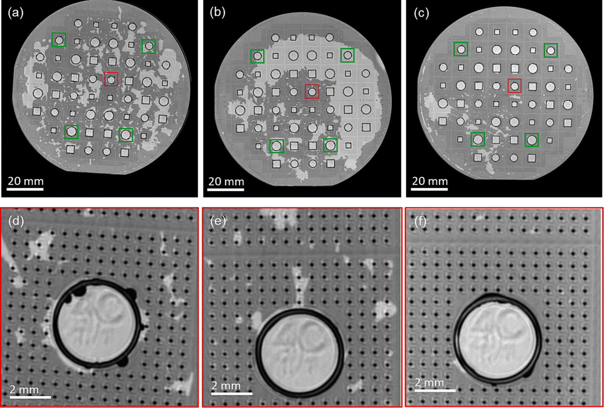
Fig. 3 shows the SAM images taken from the as-bonded wafers under water immersion. No contrast variations were observed in the microbumps and seal-ring features, which means the formed bonds were homogenous. Areas with a darker shade denote where the water permeates between the wafers. The enlargement image on the 4 mm circular seal-ring in the center area shows that the water did not penetrate through the SLID bonding, implying that the bonds are impermeable to water. Additionally, globular shapes observed next to the seal-ring show a squeeze-out formation that indicates the melting of tin‑indium.

Fig. 2. (a) Single chip model containing seal ring geometry and (b) 3D representation of a quadrant of the chip used for finite element study. In the model, atmospheric pressure was applied in the areas shaded with red colour, cavity pressure was applied at the region shaded in blue, and fixed constraints were applied at the region shaded in yellow. (c) The model meshes. (For interpretation of the references to colour in this figure legend, the reader is referred to the web version of this article.)
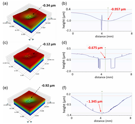
After the dicing process, the cap deflections were re-measured using a contact profilometer. Measurements conducted on four chips located close to the edge of the wafer, as marked in Fig. 3, show a maximum concave deflection of 0.93 ± 0.4 μm for Si–Si bonded at 200℃, 0.86 ± 0.5 μm for Si–Si bonded at 170 ℃, and 1.22 ± 0.3 μm for Si-Borofloat®33 bonded at 200 ℃. This shows that the hermeticity is retained through the dicing process. Fig. 4(d), (e), and (f) illustrate one of the cap deflections measured with a contact profilometer and a summary of the measurement is presented in supplementary table S2. The square-shaped dip observed in the profile comes from the RIE marking on the wafer's backside.

Fig. 3. SAM images of the samples after the bonding process: (a,b) Si–Si bonded at 200 ◦C, (c,d) Si–Si bonded at 170 ℃, and (e,f) Si-Borofloat®33 bonded at 170 ℃. Red squares indicate the seal-ring enlarged at (d, e, f) and green squares indicate the seal-rings used in cap-deflection measurements. (For interpretation of the references to colour in this figure legend, the reader is referred to the web version of this article.)

Fig. 4. The cap deflection measured in optical and contact profilometer for (a,b) Si–Si bonded at 200 ℃, (c,d) Si–Si bonded at 170 ℃, and (e,f) Si-Borofloat®33 bonded at 170 ℃.
4. Conclusions
In this study, low-temperature wafer-level SLID bonding based on Cu-Sn-In metallurgy has been successfully demonstrated using seal-ring structures. The bonding processes were conducted at temperatures as low as 170 ℃ to bond Si–Si wafer pairs and Si-Borofloat®33 wafer pairs. SAM characterization indicated that the as-bonded wafers were hermetic and have high bond quality.
This work presents a promising alternative for silicon-to-glass metal bonding for microsystem packaging. Further work should be done to further assess the package reliability, by considering several factors. First, utilizing even lower bonding temperature, given that the ternary metallurgy of Cu-Sn-In allows, to further reduce the residual stress effect. Second, utilizing larger cavities for quantitative measuring the hermeticity. Finally, implementing oxide cleaning step and improving metal stack deposition process to minimize the interface defects.