III–V solar cells are mainly grown on GaAs or Ge substrate, which significantly contributes to the final cost and affects the sustainable use of these rare materials. A so-called PEELER process is developed, in which a porosification technique is used to create a weak layer between a Ge substrate and the epitaxial layers. This method enables the separation of the grown layers, allowing for the subsequent reuse of germanium and a reduction in the environmental and economic cost of optoelectronic devices. Technology validation using the device performance is important to assess the technology interest. For this purpose, the performance of 22 nondetached single-junction GaAs photovoltaic cells grown and manufactured on porosified 100 mm Ge wafer without antireflection coating is fabricated and compared. All the cells exhibit comparable performance to stateof-the-art GaAs solar cells (grown or Ge or GaAs) with high efficiency (21.8% ±0.78%) and thereby demonstrate the viability of growing high-performance optoelectronic devices on detachable Ge films.
1. Introduction
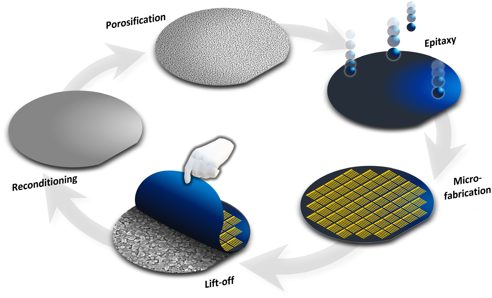
Top-performing industrial solar cells are composed of a stack of groups III–V and group IV materials (InGaP, GaInAs, Ge, GaAs, etc.) on germanium substrates These devices are costly because the component elements are rare. The substrate itself accounts for more than 30% of the cost of cell fabrication.Thus, to reduce the overall cost of these III–V and germaniumbased devices, the Ge thickness must be reduced. This can be achieved by separating the substrate and the functional layers, reducing the amount of material used in the final device. Different processes have already been developed with this aim such as spalling,selective etching, reactive ion etching (RIE)-based porosification,or van der Waals epitaxy. First developed on silicon,another promising low-cost approach consists of electrochemical porosification of the substrate followed by epitaxy and annealing (porous germanium efficient epitaxial layer release: PEELER) allowing for epilayers separation and reconditioning of the substrate. Using this method, as detailed in Figure 1, we present in this work the fabrication of III–V (GaAs) single-junction solar cells grown by metal organic chemical vapor deposition (MOCVD) on a 100 mm wide porosified germanium substrate.

Figure 1. Illustration of the main steps of the PEELER substrate reuse technique.
2. Methodology
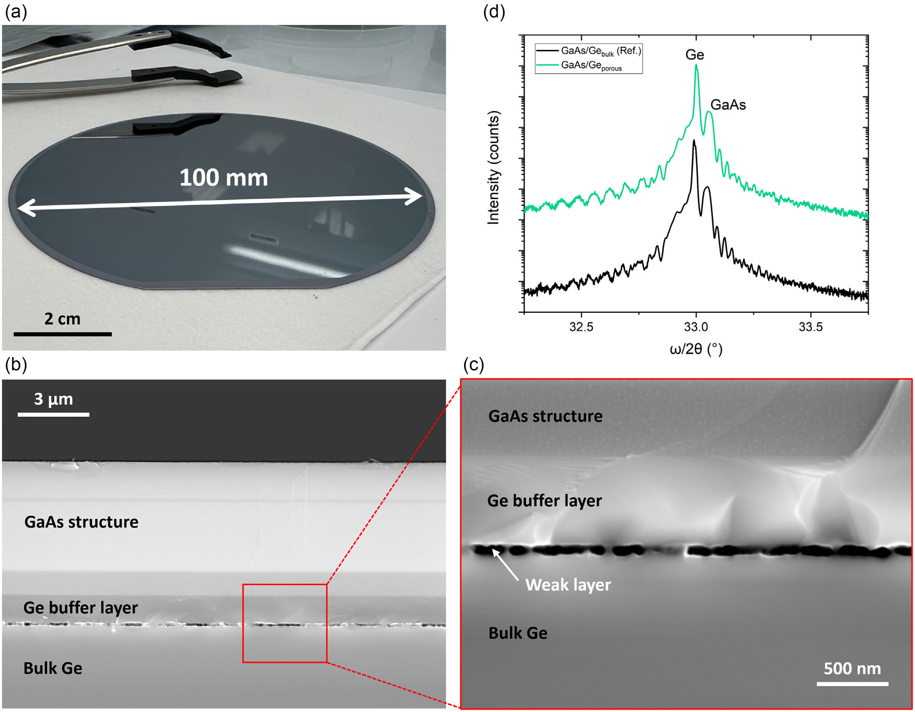
A monocrystalline Ge epitaxial layer (Gebuffer) has then been grown on the porous Ge surface. The growth has been performed following a two-step method yielding high-crystalline quality Ge membrane on a weak layer (further details on the growth process and Ge epilayer properties of this so-called PEELER process can be found elsewhere). A single-junction GaAs structure (including a 2 μm thick GaAs buffer layer) has been grown by MOCVD on this Gebuffer/Geporous/Ge wafer. In Figure 2, we can observe (a) a mirror-like surface on the monocrystalline GaAs/ Gebuffer/Geporous/Ge structure with no visible deterioration or self-delamination. Figure 2b shows a cross-sectional view of the III–V stack on the Ge template and (c) a zoom on the weak layer created after the coalescence of the pores, inducing the possibility of detaching the GaAs/Gebuffer membrane.The diffractogram presented in Figure 2d shows Ge and GaAs epilayers are both monocrystalline and comparable on bulk and porous structures.

Figure 2. a) Macroscopic and b) scanning electron microscopy (SEM) images with zoom c) of the 100 mm GaAs solar structure on Geporous restructured (weak layer) after epitaxy at high temperature, and d) the XRD ω/2θ diffractogram associated.
After the porosification of the germanium substrate and the epitaxial growth of the GaAs solar structure, we cleaved the wafer and extracted 1.5x 1.5 cm2 samples originally located at the edge and the center of the wafer. Front-contacted solar cells (represented in Figure 3a) were fabricated via three levels using our own designed photolithographic mask. The main steps include the creation of a mesa structure down to the GaAs buffer using low-damage plasma etching (a similar design reported in ref. ) and electrode metal depositions. The lift-off evaporation process for the creation of these metallic contacts has been executed by the association of different procedures.
3. Results
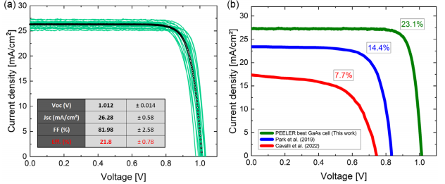
In Figure 4b, we compare the I–V characteristics of the most effi- cient nondetached GaAs cell on a PEELER substrate (presented in this study) with state-of-the-art GaAs and GaInAs singlejunction solar cells fabricated on weak layers created using analogous nanostructuring methods: the electrochemical etching and the RIE.Our best device demonstrates efficiency of 23.1%, surpassing the reported efficiencies of the best Ga(In)As cells fabricated on a detached Ge membrane through the “germaniumon-nothing” RIE-based process (eff. ref. 1 = 14.4%) or on a nondetached (bilayer) electroporosified Ge substrate (eff. ref. 2 = 7.7%). Regardless of the differences in the cells’ structures and fabrication details that may alter the overall devices’ performances, the III–V single-junction solar cells using the PEELER process show the highest reported efficiency to date.

Figure 4. a) I–V measurement of single-junction GaAs cells designed (without ARC) with mean value and b) comparison of the best one (eff. = 23.1%) with III–V single-junction solar cell fabricated on Ge wafer nanostructured with analogous techniques in the literature.
4. Conclusion
We have developed a low-cost technique for the fabrication of wafer-scale detachable optoelectronic devices on a germanium substrate (PEELER process) by using a bipolar electrochemical etching process. With this work, we demonstrate the potential of engineered substrates and their application on a 100 mm wafer for industrial compatibility (large-volume production). To validate the reproducibility of the process, the homogeneity of the material quality and the possibility of using the porosifi- cation technique for III–V photovoltaic device fabrication were investigated. 1x 1 mm2 GaAs single-junction cells of 22 fabricated on porosified germanium substrates showed high performance and small deviation (Vocmean = 1.012±0.014 V, Jscmean = 26.28±0.58 mA.cm-2 , and FFmean = 81.98±2.58%). These values are consistent with those expected for GaAs solar cells on conventional Ge substrate nonporosified. The best cell of this batch has an efficiency of 23.1%, higher than the reported values of the current literature on detachable germanium films. This demonstrates experimentally that the PEELER process can yield materials with device quality. These results also demonstrate the compatibility of the porous structure with MOCVD growth and thus confirming the industrial potential of this method, opening the path toward detachable multijunction solar cells and other applications. Further development for the detachment of thin solar cells will be continued to enable multiple reuses of the Ge substrates.