This work studies the impact of the silicon (Si) loading effect induced by deep reactive ion etching (DRIE) of silicon master molds on the UV-nanoimprint lithography (NIL) patterning of nanofeatures. The silicon molds were patterned with metasurface features with widths varying from 270 to 60 nm. This effect was studied by focus ion beam scanning electron microscopy (FIB-SEM) and atomic force microscopy (AFM). The Si loading etching effect is characterized by the variation of pattern feature depth concerning feature sizes because smaller features tend to etch more slowly than larger ones due to etchants being more difficult to pass through the smaller hole and byproducts being harder to diffuse out too. Thus, the NIL results obtained from the Si master mold contain different pattern geometries concerning pattern quality and residual photoresist layer thickness. The obtained results are pivotal for NIL for fabricating devices with various geometrical nanostructures as the research field moves towards commercial applications.
1. Introduction
Developing low-cost high-throughput nanolithography techniques with high resolution is essential for commercialisation applications. Due to its ability to transfer patterns with a wide variety of geometry and size without compromising mass manufacturability, nanoimprint lithography (NIL) has attracted considerable attention over the past few years. This technique opens the way for many applications not just in the microfabrication industry but also in the industry of nanodevices.
NIL has been identied by the International Technology Roadmap for Semiconductors (ITRS) as a potential nextgeneration lithography technique alongside conventional UVphotolithography, e-beam lithography (EBL), and extreme UV lithography (EUVL).5 The resolution limit of current UVphotolithography stands at approximately ∼10 nm half pitch for lines and spaces, which can be achieved with increased production costs due to additional etching and deposition steps involved in pitch splitting.6 E-beam lithography, a direct writing technique, offers lower throughput than industry standards and ITRS. Meanwhile, extreme UV lithography (EUVL) using equipment operating at a 13.5 nm wavelength coupled to a 0.55NA lens is expected to enable patterning a 10 nm half-pitch by 2025.7 However, the main challenge lies in the substantial changes required to upgrade the system, including a higher numerical aperture (NA) or a shi to a shorter wavelength,necessitating a new light source system, multilayer coating, and potentially a new photoresist.
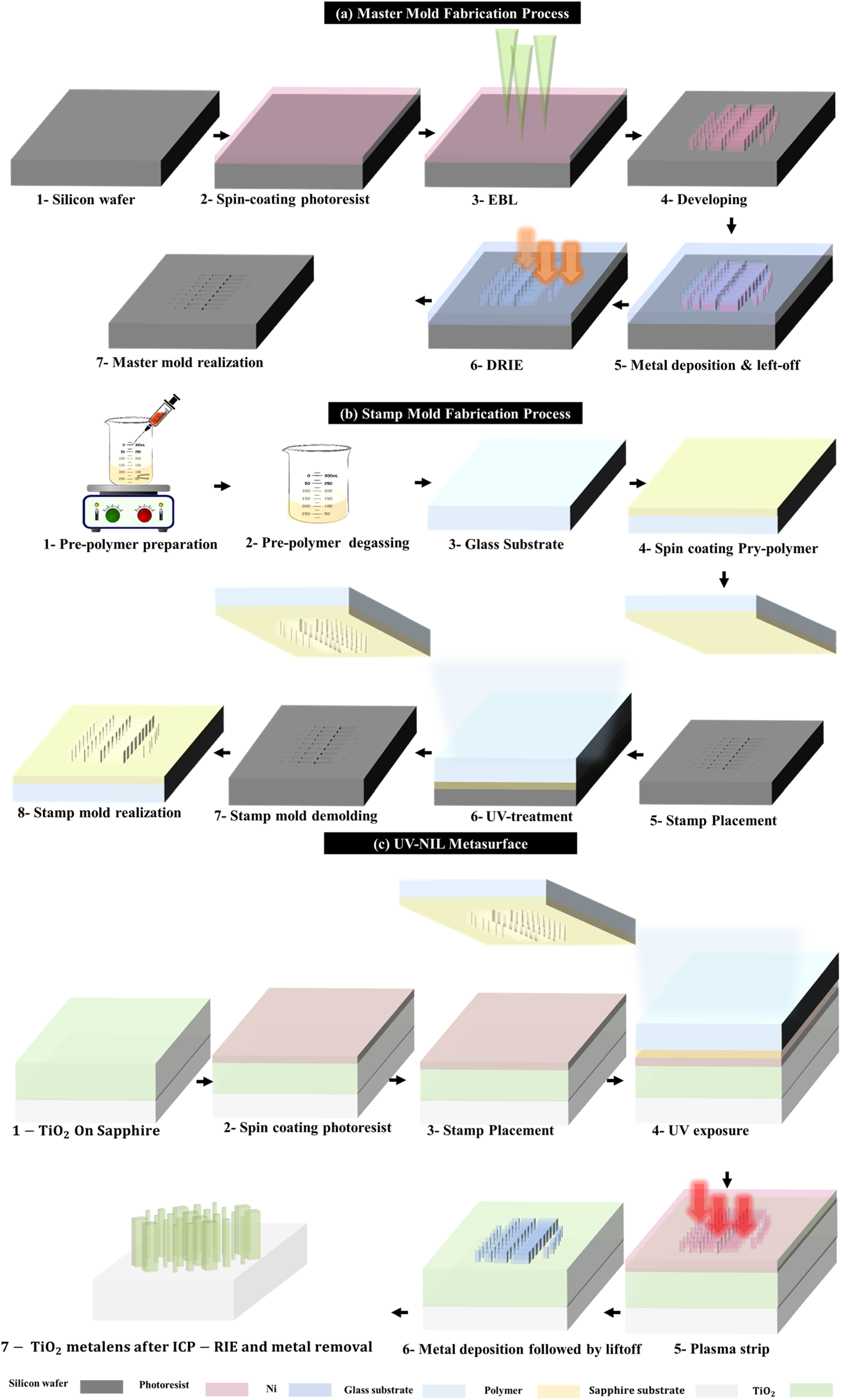
UV-nanoimprint lithography (UV-NIL) distinguishes itself in the field of lithography by utilizing ultraviolet light to achieve pattern replication through a methodical process comprising four dened stages. Initially, the process begins with the creation of a master mold, employing advanced techniques such as EBL, X-ray lithography, focused ion beam (FIB), or EUVL to establish the pattern to be replicated. Following this, the replication surface is prepared by coating a glass wafer with a liquid exible polymer, which is then solidied through either thermal curing or UV light exposure, setting the stage for pattern transfer. The third step involves the imprinting phase, where a photoresist layer is applied to the substrate and the patterned transparent stamper mold is pressed against it. This assembly is then exposed to UV light, ensuring the transfer of the pattern by curing the photoresist. The final stage concludes the process by carefully separating the stamper mold from the substrate and removing any residual layers on the substrate with an oxygen plasma process, thereby revealing a awlessly replicated pattern. This structured approach not only highlights UV-NIL's unique position in lithography but also showcases its efficiency and precision in pattern replication.
2. Materials and methods
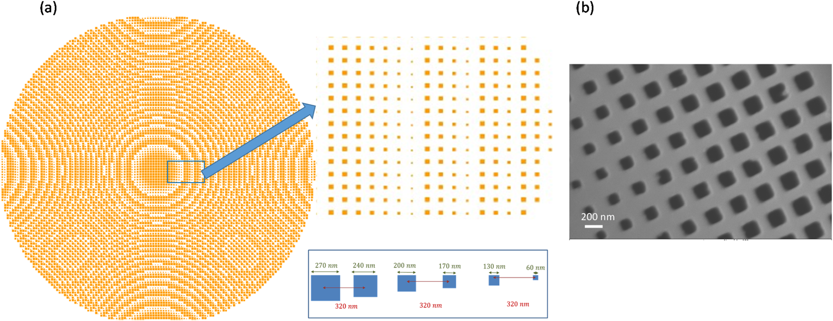
The study is based on the direct-imprint UV-NIL method, where a stamp inverts a master's patterns, which are subsequently reinverted into the imprint material to recreate the master's original structure of a metasurface device, which is based on a special arrangement of TiO2 square pillars. The design structure is schematically illustrated in Fig. 1. It consists of TiO2 square pillars on the front of a sapphire substrate. The target geometries are found from the maximum amount of the transmitted electromagnetic beam with ld = 633 (nm) (for more information check our earlier work35). They are found to be: height (h) = 600 (nm) length (l) = (0 to 270) (nm) and cell size (p) = 320 (nm).

Fig. 1 Illustration of the metasurface structure illustrating a special arrangement of square with varying length and (b) scanning electron microscopy (SEM) image of the fabricated NIL master mold with a metasurface pattern on silicon.
The selection between Bosch DRIE and cryogenic DRIE for optical device fabrication hinges on the specic outcomes sought from our production process. Cryogenic etching tends to yield patterns with signicant surface roughness around the openings, leading to highly irregular opening shapes, whereas Bosch etching results in smoother openings at the top. Because with prolonged etching time, the mask layer can degrade faster due to the drop in temperature of the substrate given our particular application needs, Bosch DRIE emerges as the optimal choice due to its effectiveness and cost efficiency, aligning closely with our project's requirements.
Finally, the entire setup was exposed to UV light from a mercury vapor lamp for 15 minutes, curing the polymer and solidifying the pattern onto the glass. The system was then left to stabilize at room temperature overnight before the newly formed stamp mold was carefully separated from the master mold. This intricate process ensured the creation of a highquality stamp mold, ready for use in transferring nano-scale patterns onto substrates.
Fabricating metasurfaces with UV-NIL is a methodical process, structured into three principal steps. Initially, titanium dioxide (TiO2) is deposited onto a 2-inch sapphire substrate using electron beam evaporation (EBE), creating a foundational layer crucial for the subsequent steps. This process, particularly the deposition and resulting optical properties of the 600 nm TiO2 thin film, is detailed further in our previous work. An illustrative overview of the entire UV-NIL patterning process is provided in Fig. (2).

Fig. 2
3. Results and discussion
3.1 Master mold fabrication and silicon loading effect
The successful realization of the nano-pattern features of the UV-NIL metasurface is highly dependent on the etching profile of the silicon master mold. Among all techniques of RIE processes, the Bosch DRIE process for silicon that involves repetitive passivation and etching cycles enables the etch process to proceed deeper into the substrate with a small tapping angle.The first step of the etching process is the deposition of an etching-resistant polymer layer (C4F8) over the entire substrate surface. The deposition of the polymer prevents the sidewalls from being etched; thus, nano-holes with vertical sidewalls in the silicon wafer are obtained. Next, the polymer layer on the bottom of the hole is removed by bombarding ion plasma to clear the surface for the etchant gas reactive species to interact with silicon atoms. In the last step of the process, (SF6) is introduced into the silicon substrate for a short time. Then the flow of (C4F8) process gas starts the deposition coating of the passivation polymer before etching further.
Interestingly, our characterization revealed that the FWHM remained constant at 0.52 mm across the three metasurfaces, suggesting that the precision in focusing, as determined using the FWHM, remained consistent. However, a notable variation was observed in the intensity of the focused beam among the metasurfaces. This difference in intensity, despite a uniform FWHM, underscores the complexity of optical interactions within metasurfaces and highlights the importance of comprehensive characterization. This suggests that while the ability to concentrate light to a tight focal spot may be consistent, the efficiency with which light is focused—and thus the overall optical efficiency of the metasurfaces—can vary, impacting their suitability for different applications.
4. Conclusion
In this work, we delved into the profound impact of the silicon loading effect, stemming from the deep reactive ion etching (DRIE) of silicon master molds, on the UV-nanoimprint lithography (NIL) patterning of nanofeatures crucial for metalens design aimed at focusing incident laser beams at a specified focal spot. This exploration spanned the intricate stages of UVNIL for metalens fabrication, examining how the silicon loading effect influences both the master mold's integrity and the subsequent successful removal of the residual photoresist layer. Our findings illustrated the pivotal role of stamp S-MM3, selected for its ability to overcome the challenges that hindered the pattern transfer in stamps S-MM1 and S-MM2, thereby underscoring the necessity for complete yet precise removal of the residual layer to avoid over-etching.