High-performance organic phototransistors (OPTs) have attracted considerable attention owing to their high photoresponse and low-cost solution-processing manufacturing. To meet the increasing demand for integrated optoelectronic circuits, organic single-crystalline micro-/nanowire arrays for OPTs construction are prominently anticipated. However, the manufacturing and patterning of organic single-crystalline arrays have hit a bottleneck due to the uncontrollable dewetting dynamics. In this work, a capillary-bridge lithography strategy is proposed to guide ordered nucleation and unidirectional dewetting of microfluid, thus enabling the large-scale preparation of highly aligned organic single-crystalline microwire arrays. Taking advantage of efficient carrier transport, a competitive average field-effect hole mobility (𝝁) of 6.64 cm2 V−1 s−1 is obtained, and the high-throughput one-dimensional (1D) arrays based OPTs also exhibit excellent optoelectrical performance with photosensitivity (P) of 1.36 × 10⁶, responsivity (R) of 3.18 × 10⁴ A W−1, and specific detectivity (D*) of 9.22 × 10¹⁴ Jones. This work provides a guide for the designing and patterning of high-throughput OPTs toward multifunctional integrated optoelectronics.
1. Introduction
The efficient detection of optical information plays an important role in modern science and technology. With the advantages of tunable bandgap, mechanical flexibility, and low-cost and solution-processing manufacturing of organic semiconductor materials served as photoactive layers, organic photodetectors have attracted considerable attention and showing great potential in next-generation image sensors, health monitoring, quantum communication, biomedical sensing and so on. As a typical photo-sensor for highly sensitive photodetection, OPTs in which the channel carrier density can be effectively modulated by both gate voltage and incident light, exhibit higher sensitivity, intrinsic amplification, and lower dark currents compared with the traditional two-terminal photodiodes, thus boosting a series of advanced research.
Herein, we present a capillary-bridge lithography strategy for efficient large-scale patterning of 6,13-bis (triisopropylsilylethynyl)pentacene (TIPS-PEN) single-crystalline microwire arrays. With the assistance of asymmetric-wettability micropillar templates to manipulate the nucleation and orientated growth of organic crystal, high-quality single-crystalline 1D microarrays with strict alignment, homogeneous size, and ordered crystallographic packing can be successfully fabricated. The synergy of single-crystalline nature and the optimal packing orientation resulted in high average hole mobility of 6.64 cm2 V−1 s−1and low dark current of organic field effect transistors (OFETs) based on the TIPS-PEN single-crystalline 1D microarrays. As a result, microwire array OPTs showed a superior optoelectrical characteristics with P of 1.36 × 10⁶, R of 3.18 × 10⁴ A W−1, and D* of 9.22 × 10¹⁴ Jones compared to their polycrystalline film counterparts. Our work provides a new platform for constructing high-performance phototransistors, and accelerating the development of integrated optoelectronics.
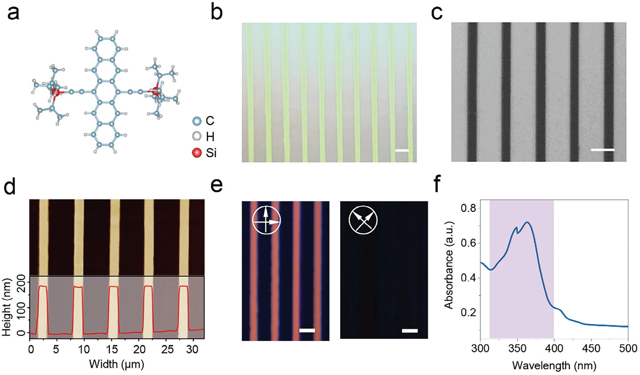
To evaluate the quality of the fabricated TIPS-PEN (Figure 1a) 1D microwire arrays, a systematic characterization of morphology and crystallography were performed. As shown in Figure 1b and Figure S7 (Supporting Information), the optical microscopy images present highly ordered organic microwire arrays with homogeneous morphology over the large area. The scanning electron microscope (SEM) was employed to further demonstrate the high crystallinity of ordered organic microwire arrays with strict alignment, controlled position, and homogeneous size (Figure 1c). Zoom-in SEM image further manifests that the single microwire possesses a smooth surface and straight boundary (Figure S8, Supporting Information). The corresponding energy dispersive spectrum (EDS) mappings of the TIPS-PEN microwire arrays present the homogeneous distribution of C and Si elemental elements. A typical atomic force microscopy (AFM) in Figure 1d illustrates the ordered organic microwire with smooth surfaces and sharp edges, 190.2 nm in height, and 1.9 μm in width, confirming high-quality organic microwire arrays. Figure 1e displays the parallel-polarized and cross-polarized optical microscopy of microwire arrays observed by polarization microscopy. As the polarization angle rotates from 0° to 45°, all 1D crystals extinguished cross-polarized fluorescence simultaneously, reflecting the single-crystalline property of the long-range ordered microwire arrays with pure crystallographic orientation. The ultraviolet–visible (UV–vis) absorption spectrum of TIPS-PEN single crystal is displayed in Figure 1f, showing an intense absorption peak at 365 nm.

Figure 1. a) The molecular structure of TIPS-PEN. b) In situ optical microscopy image of TIPS-PEN 1D microwire arrays. c) SEM image and d) AFM image and height diagram of 1D arrays. e) The cross-polarized optical microscopy of 1D arrays, indicating the single-crystalline nature. f) The UV–vis absorption spectra of TIPS-PEN single crystal. Scale bars in (b,c,e): 5 μm.
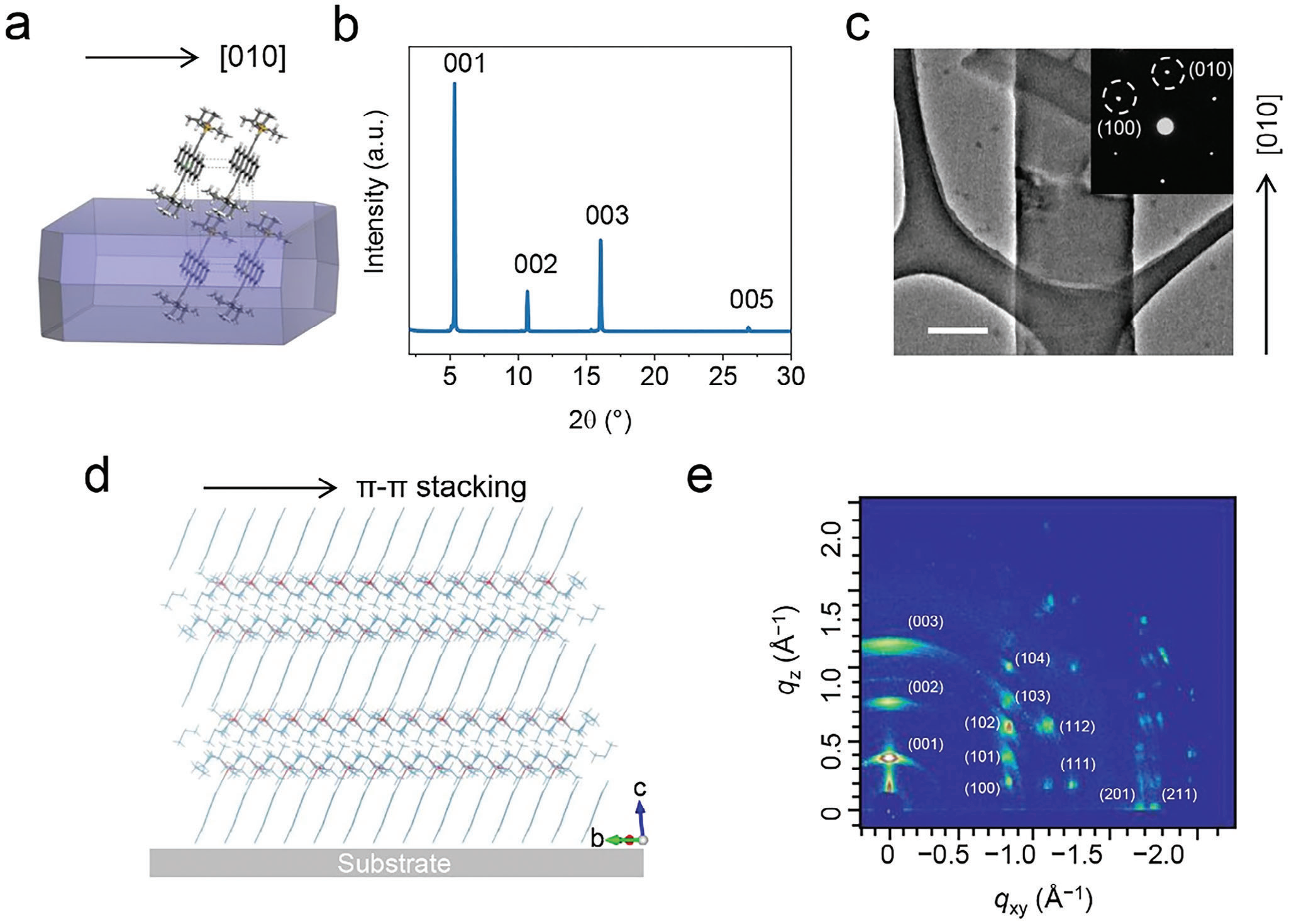
The crystal morphology prediction is obtained by BFDH (Bravais–Fridel and Donnay–Harker) algorithm. The predicted crystal morphologies reveal the preferred orientation [010] in the crystal shape (Figure 2a). To verify this prediction, we carried out X-ray diffraction (XRD), transmission electronic microscopy (TEM), selected area electron diffraction (SAED) and grazingincidence wide-angle X-ray scattering (GIWAXS) to examine the in-plane and out-of-plane orientations of TIPS-PEN microwire arrays. Figure 2b displays the out-of-plane XRD pattern with smooth baseline and sharp diffraction peaks, indicating the high crystallinity of microwire arrays. According to the data simulated from the bulk crystal, the primary diffraction peak at 5.33° is well assigned to (001) diffraction peak, while the multi-order diffraction peaks at 10.67°, 16.03°, and 26.86° corresponding to (002), (003), and (005), respectively, reflecting that the ab plane of microwire arrays is parallel to the substrate (Figure 2b,d). As shown in Figure 2c, TEM image reveals a smooth surface and sharp edge of individual microwire, and the sharp and discrete diffraction spots can be observed in the corresponding SAED pattern, verifying the single-crystalline nature of microwire. Combining the TEM and SAED results with the crystal structure data of TIPS-PEN, it is clear that the microwires grow along with the orientation, coinciding with the direction of molecular packing, which is favorable for the hole transport (Figure 2d).As presented in Figure 2e, the sharp and discrete diffraction Bragg spots can be clearly seen in GIWAXS pat tern, which is further confirmed the high crystallinity of highly ordered microwires and the out-of-plane direction of crystal orientation. Therefore, the TIPS-PEN 1D arrays fabricated by capillary-bridge lithography strategy were demonstrated with intrinsically defect-free single-crystalline nature, which would facilitate the in-plane carrier transport and quality contact between the microwires and the electrodes for high-performance devices with high mobility.

Figure 2. a) Calculated crystal growth morphology of the TIPS-PEN. b) XRD pattern of 1D arrays, revealing the (001) out-of-plane direction. c) TEM image of an individual microwire and the corresponding SAED pattern, suggesting a [010] growth direction of 1D single-crystalline microwire. Scale bar: 1 μm. d) Out-of-plane molecular packing of TIPS-PEN crystal with ab plane parallel to the substrate. e) GIWAXS image of 1D arrays, verifying the (001) out-of-plane direction.
3. Conclusion
In summary, we have developed a capillary-bridge lithography strategy for patterning TIPS-PEN 1D single-crystalline microwire arrays with controlled geometry, position, and size in large area. The fabricated 1D arrays feature high crystallinity and ordered crystallographic alignment, promoting the charge transport ef ficiency. The corresponding 1D array based OFETs show an excellent electrical performance with high average hole mobility of 6.64 cm2 V−1 s−1. Encouraged by the significantly improved mobility and reduced dark current, high-performance OPTs were successfully achieved with high photoresponse with P of 1.36 × 10⁶, R of 3.18 × 10⁴ A W−1, and D* of 9.22 × 10¹⁴ Jones, which are superior to the corresponding film-based devices. We believe these results are likely to provide a promising platform for single-crystalline array phototransistor in future developments of multifunctional integrated optoelectronics.
4. Experimental Section
Fabrication of Topographical Templates: N-doped silicon wafers with diameter of 10 cm, thickness of 525 μm, and <100> orientation were used as template carriers. To fabricate periodic micropillar-structure substrates, a direct laser writing apparatus (Heidelberg DWL200) was adopted to transfer the computer predefined design onto the photoresist (Shipley Microposit S1800 series) coated wafers with ≈1 μm precision, then followed by UV irradiation and etching with fluorine-based reagents using deep reactive ion etching (Alcatel 601E). After resist stripping (Microposit Remover 1165) and cleaning with acetone and ethanol, the topographical templates possessed periodic micropillar structures with width of 2 μm, height of 20 μm, and adjacent distance of 5 μm were obtained.
Selective Modification of Topographical Template with Asymmetric Wettability: The template was first cleaned with acetone, ethanol, and deionized water, followed by oxygen plasma for ≈10 min. Then a flat silicon substrate with spin-coated thin film of SU-8 was pressed onto the micropillar template. After SU-8 curing at 95°C, the silicon substrate was peeled off, leaving a SU-8 film covered on the lyophilic micropillar tops. The top-protected micropillar template was further modified by heptadecafluorodecyltrimethoxysilane molecules with low surface energy, giving rise to the lyophobic sidewalls of micropillars. After removing the SU-8 protection film, the asymmetric-wettability topographical template was fabricated.
上一篇: 硅中的负载效应对超透镜纳米级图案的影响