Abstract
Superconducting circuits based on hybrid InAs Josephson Junctions (JJs) play a starring role in the design of fast and ultra-low power consumption solid-state quantum electronics and exploring novel physical phenomena. Conventionally, 3D substrates, 2D quantum wells (QWs), and 1D nanowires (NWs) made of InAs are employed to create superconductive circuits with hybrid JJs. Each platform has its advantages and disadvantages. Here, we proposed the InAs-on-insulator (InAsOI) as a groundbreaking platform for developing superconducting electronics. An epilayer of semiconductive InAs with different electron densities was grown onto an InAlAs metamorphic buffer layer, efficiently used as a cryogenic insulator to decouple adjacent devices electrically. JJs with various lengths and widths were fabricated employing Al as a superconductor and InAs with different electron densities. We achieved a switching current density of 7.3 μA/μm, a critical voltage of 50-to-80 µV, and a critical temperature equal to that of the superconductor used. For all the JJs, the switching current follows a characteristic Fraunhofer pattern with an out-of-plane magnetic field. These achievements enable the use of InAsOI to design and fabricate surface exposed Josephson Field Effect Transistors with high critical current densities and superior gating properties.
Introduction
Superconducting circuits based on Josephson Junctions (JJs) play a starring role in the design of fast and ultra-low power consumption solid-state quantum electronics. Over the last decades, hybrid superconductor-semiconductor JJs have attracted growing interest as basic blocks to explore novel physical phenomena and to build quantum electronic architectures . Various applications have been documented, encompassing gate-tunable superconducting and Andreev qubits, superconducting transistors, diodes , and interferometers. These applications extend to quantum phenomena such as spin dependent supercurrent, topological phase transitions, anomalous phase shifts in ground state , and parity-protected systems.
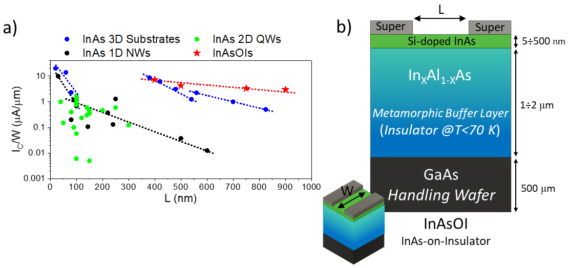
JJs and gate-tunable JJs, also known as Josephson Field Effect Transistors (JoFETs), were initially reported by Takayanagi et. al. in 3D InAs substrates featuring surface 2-dimensional electron gases (2DEGs) . Increasing the InAs bulk electron density correlated with a rise in the critical current density of the Josephson junction (IC/W, where W represents the junction width), achieving the notable value of 20 μA/μm for a junction length (L) of 20 nm with Nb electrodes (Figure 1a, blue dots, Table S1). However, practical implementations of this platform face obstacles due to the lack of an insulating layer between adjacent devices, which is linked to the conductivity of the InAs substrate.

Figure 1
The surface-exposed InAs epilayer supports a non-dissipative current via the superconductingproximity-effect inherited by the superconducting leads, e.g., Al , Pb, Nb , NbTi , and others . The presence of InAs on the top of the structure allows direct access to the final semiconductive channel, where its electronic transport properties can be tuned, changing the InAs doping during (via atoms incorporation) or post (via dopants implantation or thermal diffusion) the heterostructure growth. The μm-thick InAlAs metamorphic buffer layer avoids lattice mismatch between the InAs and the GaAs handling substrate and can be employed as an insulator at cryogenic temperature. Regardless of the fabrication technique, which is typical of GaAs-based heterostructures, the InAsOI represents the superconducting twin of the silicon-on-insulator (SOI) architecture, where proximitized InAs and the cryogenic insulating InAlAs replace silicon and silicon oxide layers of SOI, respectively.
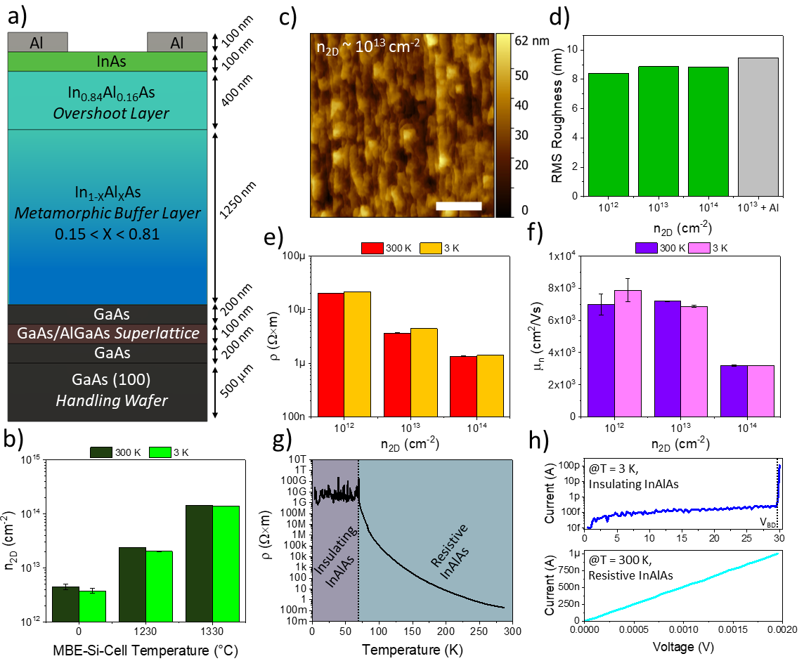
We then evaluated the temperature-dependent electrical behavior of the InAlAs metamorphic buffer by measuring the layer resistivity. As shown in Figure 2g, ρ increases from ~ 100 mΩ×m at 300 K to 10 GΩ×m at 70 K, below which it remains unchanged. Figure 2h shows current vs. voltage (I-V) curves of an InAlAs strip (200 μmwidth and 5 μm length) recorded both at 300 K and 3 K. At room temperature, the InAlAs exhibits a resistive behavior (Figure S5) with a linear I-V characteristic and a resistance of ~ 2 kΩ. On the other hand, at 3 K, the metamorphic buffer layer shows an insulating behavior with an apparent breakdown voltage (VBD) of 30 V and a parallel resistance before the avalanche breakdown of 140 TΩ. The latter result indicates that the metamorphic buffer layer can be efficiently used as an insulator for temperatures lower than 70 K, which is well above every BCS superconductor's critical temperature (Tc).

Figure 2
We then evaluated the temperature-dependent electrical behavior of the InAlAs metamorphic buffer by measuring the layer resistivity. As shown in Figure 2g, ρ increases from ~ 100 mΩ×m at 300 K to 10 GΩ×m at 70 K, below which it remains unchanged. Figure 2h shows current vs. voltage (I-V) curves of an InAlAs strip (200 μm width and 5 μm length) recorded both at 300 K and 3 K. At room temperature, the InAlAs exhibits a resistive behavior (Figure S5) with a linear I-V characteristic and a resistance of ~ 2 kΩ. On the other hand, at 3 K, the metamorphic buffer layer shows an insulating behavior with an apparent breakdown voltage (VBD) of 30 V and a parallel resistance before the avalanche breakdown of 140 TΩ. The latter result indicates that the metamorphic buffer layer can be efficiently used as an insulator for temperatures lower than 70 K, which is well above every BCS superconductor's critical temperature (Tc).
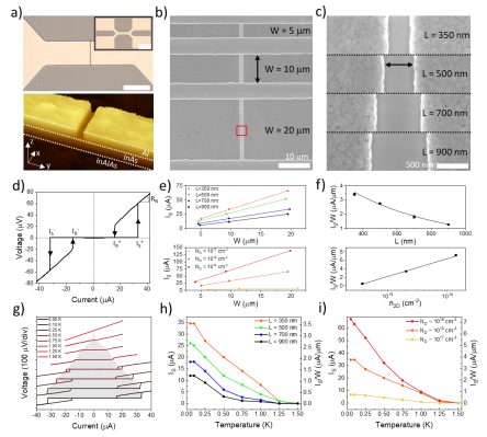
We realized superconductor-semiconductor-superconductor Al-InAs-Al JJs with several widths (W = 5, 10, 20 μm) and inter-electrode separations (length, L = 350, 500, 700, 900 nm), using InAsOIs with different InAs sheet electron densities. Devices were fabricated via two aligned lithographic steps: first, Al and InAs MESA were defined by UV-lithography and manufactured by successive Al and InAs wet etching, setting the JJ width and leaving the cryogenic-dielectric-InAlAs layer exposed. Then, the JJ length was defined by electron-beam-lithography and Al wet-etching, leaving the underneath InAs unaffected. Figure 3a top shows an optical microscopy image of a JJ featuring a width of 20 μm and a length of 900 nm (chosen to emphasize the interelectrode separation). In contrast, the inset shows the whole device. A clear separation between the light-grey area (Al-area) and the dark-gray area (MESA etched area) is observed in the picture, with straight edges related to fine-controlled etching during device processing.

Figure 3
Conclusions
In this work, we proposed the InAs-on-insulator (InAsOI) as a groundbreaking platform to develop superconducting electronics. An epilayer of semiconducting InAs with different electron densities was grown onto an InAlAs metamorphic buffer layer, efficiently used as a cryogenic insulator to electrically decouple adjacent devices. Josephson Junctions with various lengths and widths were fabricated using Al as a superconductor and InAsOI with different electron densities. The switching current and supercurrent density can be easily tuned by orders of magnitude by changing both the JJ morphological properties and the InAs electron density. We achieved a switching current density of 7.3μA/μm, a critical voltage of 50-to-80 µV, and a critical temperature equal to that of the superconductor used. For all the JJs, the switching current follows a characteristic Fraunhofer pattern with the out-of-plane magnetic field, from which a switching current suppression factor of 99.95 % was calculated. These achievements open up the use of the InAsOI platform to design and fabricate surface-exposed Josephson Field Effect Transistors with high critical current densities and superior gating properties. Moreover, the electron density of the InAs epilayer can be locally tuned post-heterostructure growth via dopant implantation or thermal diffusion to obtain quantum devices with different properties on the same substrate.