ABSTRACT
In this work a multilevel nanoimprint lithography (NIL) replication process was demonstrated to produce 1D MEMS mirrors employing vertical asymmetric comb-drive electrostatic actuation, in a 200 mm wafer SOI-based process. In comparison with a direct write laser (DWL) grayscale lithography step (which for the proposed layout requires around 40 h of exposure time per wafer), this NIL method greatly enhances fabrication throughput by reliably reproducing a master's multilevel topography onto the photoresist. This study describes the NIL master fabricated using grayscale lithography, the working stamp, and the replication micromachining processes. An extensive characterization of the morphology and topography of the intermediate working stamp is provided, along with an optimization study of the replica fabrication and the alignment procedure between the replica and the mirror substrate. The MEMS device pattern was effectively replicated, exhibiting electrode gaps of 3.66 μm (grayscale process yields gaps of 3.5 μm). Discrete photoresist levels of 1.53 μm and 2.83 μm were observed, with a misalignment to the preceding metal layer of 5 μm and 10 μm in the x and y directions, respectively. These deviations were found to be within the required alignment margin defined by the layout (20 μm). The 1D MEMS mirror fabricated using this NIL process was successfully characterized using Scanning Laser-Doppler Vibrometry under atmospheric pressure conditions. The results obtained were in accordance with the theoretical design parameters, demonstrating that NIL can be successfully used as a fast, low-cost alternative lithography process to fabricate multilevel MEMS structures.
1. Introduction
MEMS (Micro-electro-mechanical Systems) technologies have found widespread applications across various industries, from automotive to consumer electronics, with the added advantage of batch microfabrication. MEMS devices fabricated through surface and bulk micromachining techniques typically involve a sequence of lithography and etching steps to pattern and shape the electromechanical microstructures precisely. However, the correct alignment between each lithography step can often present a challenge, being extremely crucial for the viability of the final devices, especially in devices with very narrow electrode gap tolerances.
One MEMS device that presents this constraint is the MEMS mirror based on vertically asymmetric comb electrodes, i.e., electrodes with thickness asymmetry on a single silicon layer. The fabrication of these actuators typically relies on the use of several lithography steps to define the discrete mask levels using different materials, as presented in, or using two layers of the same material defined in different lithographic processes, as in. These are often prone to misalignments between actuators, which may arise due to the resolution of the system camera or from the alignment marks quality, among others. When designing a device with a minimal electrode gap (smaller than 3 μm given a 50 μm SOI layer), this misalignment can compromise the final device performance or process yield.
2. Materials and methods
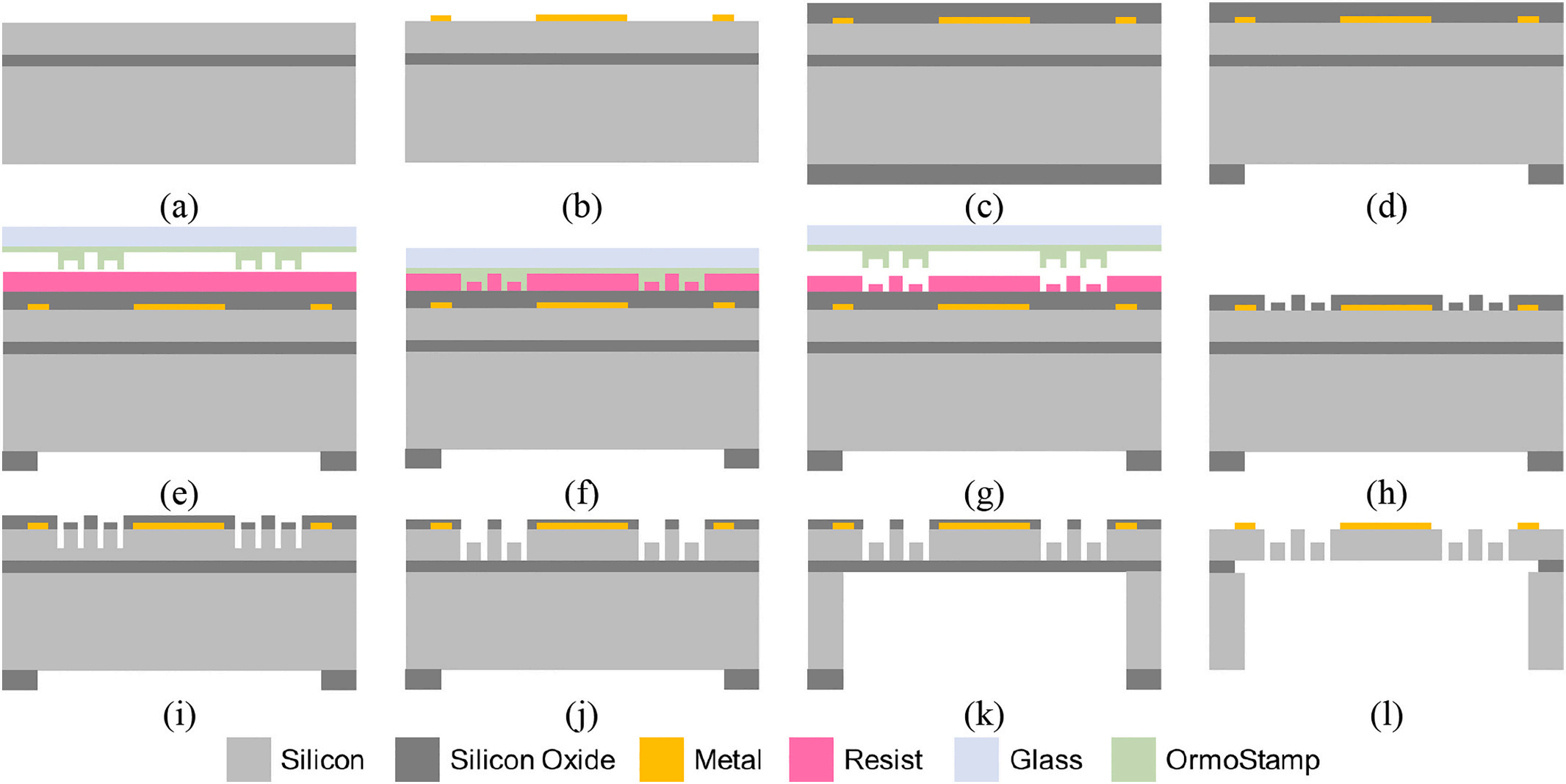
The multilevel micromachining process with NIL is based on the work presented in, as described in Fig. 1. Here, the MEMS mirrors, are fabricated on a 50 μm-thick Silicon-on-Insolator (SOI) double-side polished wafer, where initially a 500 nm-thick layer of an aluminium alloy, AlSiCu (which is composed of a large percentage of aluminium, 98.5 %, and a small one of silicon and copper, 1 % and 0.5 %, respectively) is sputtered and patterned (Fig. 1b) to create the mirror reflective surface, the electrical contacts and the alignment marks for the subsequent processes. Then, a thick layer of silicon oxide (SiO2) is deposited, by Chemical Vapor Deposition (CVD), on the wafer frontside and on the backside, with thicknesses of 3 μm and 5 μm, respectively, working as hard-masks (Fig. 1c). The handle pattern is then transferred to the backside oxide layer by reactive ion etching (RIE) to create the MEMS mirror cavity (Fig. 1d). At this stage, the multilevel patterned design, comprising three distinct levels, is exposed on the frontside using the proposed NIL step using a master stamp (Fig. 1e–g).

Fig. 1. 1D MEMS mirror micromachining process main steps, where (a) SOI wafer preparation; (b) AlSiCu layer deposition and patterning; (c) SiO2 hard-masks deposition; (d) backside hard-mask RIE; (e) frontside resist coating and stacking of SOI wafer and NIL stamp; (f) stamp filling and curing; (g) demolding; (h) multilevel pattern transfer to hard-mask layer; (i) frontside 1st DRIE step; (j) frontside mask thinning and 2nd DRIE step; (k) backside DRIE; and (l) structure release by HF vapor.
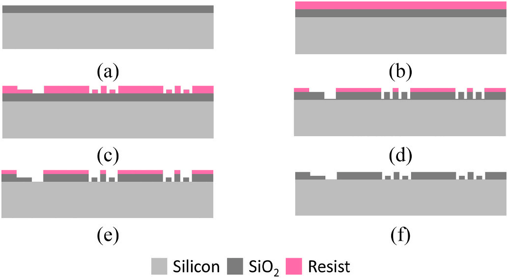
The NIL silicon master contains the same multilevel pattern to be positively replicated onto the frontside of the 1D MEMS mirror. The master was micromachined by combining grayscale lithography and silicon RIE onto a 200 mm single side polished wafer, as depicted in Fig. 2. Here, a thin AZP4110 (from Microresist) photoresist layer with a thickness of 2.2 μm was uniformly coated onto the wafer surface. The photoresist layer was subsequently grayscale exposed with the MEMS mirror and asymmetric comb electrodes pattern, which presented a final thickness after the development of 0 μm (maximum grayscale level), 1.1 μm (medium grayscale level) and 2.2 μm (null level). This exposure is a critical step in the MEMS mirror micromachining process, as previously detailed, to create the perfectly aligned asymmetric electrostatic electrodes which will induce a torque in its reflective movable structure, to steer a laser beam.

Fig. 2. Multilevel silicon master micromachining process main steps, where (a) SiO2 CVD; (b) photoresist spin coating; (c) grayscale lithography; (d) 1st SiO2 RIE etching step, followed by PR mask thinning; (e) 2nd SiO2 RIE etching step to half of the initial thickness; and (d) PR mask cleaning.
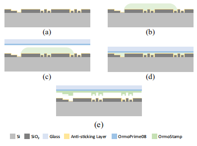
The proposed NIL process uses an intermediate working stamp with the negative replica of the master structures. After the successful fabrication of the master, the subsequent phase involved the creation of an intermediate working stamp which is a negative replica of the master, illustrated in Fig. 3. For this purpose, UV curing NIL, using the Eitre® 8 system from Obducat, was employed.

Fig. 3. Intermediate working stamp micromachining process main steps: (a) master anti-sticking treatment; (b) OrmoStamp disposal onto the Si master; (c) placing the glass substrate with adhesion promotor OrmoPrime08 on top of OrmoStamp; (d) OrmoStamp moulding and curing; and (e) demolding.
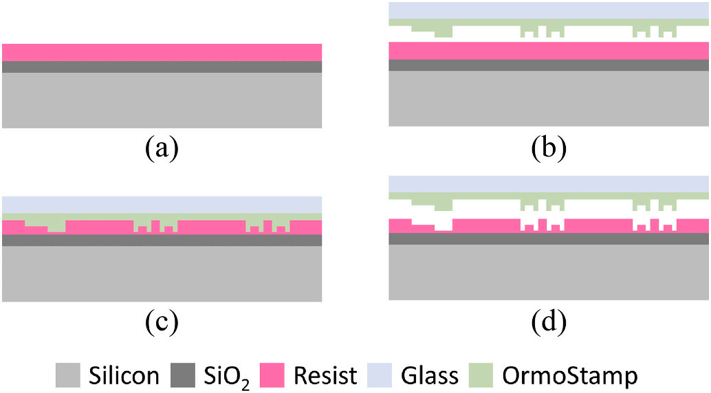
Prior to the NIL process, the intermediate working stamp was also coated with a fluorinated anti-sticking layer. The replication process follows the process flow depicted in Fig. 4. Once again, the stack composed of the Si wafer with a SiO2 layer and resist (Fig. 4a), and the intermediate stamp was manually prepared.

Fig. 4. Multilevel replica micromachining process main steps, where (a) photoresist spin coating; (b) stacking of replica wafer and stamp; (c) stamp filling and curing (d) separation.
3. Results & discussion
3.1. Intermediate working stamp quality
In order to provide a closer examination of the intermediate working stamp, scanning electron microscopy (SEM) was performed, enabled by a 10 nm thickness gold layer deposited on it. The resulting images (Fig. 5) show the negative of the expected MEMS mirror features. The specific layout details as well as the three distinct levels of the replicated microstructures on the stamp can be observed. The features edges present a high quality vertical wall. Some roughness on the etched lowleveled silicon can be observed, however this is enlarged due to the gold layer, and does not have an impact on the NIL replica and subsequent micromirror performance.

Fig. 5. Device layout and SEM images of the intermediate working stamp (with 10 nm-Au coating).
4. Conclusions
This work presents a novel approach using NIL replication to fabricate multilevel self-aligned structures in a more efficient and costeffective manner, tailored in this particular case for MEMS mirrors with asymmetric electrodes on a 200 mm wafer. This method typically utilizes DWL grayscale lithography to achieve the desired multilevel pattern, which traditionally requires approximately 40 h per wafer for exposure (on the DWL Heidelberg 2000). However, by implementing and optimizing NIL for batch production, we demonstrated that the process time was significantly reduced, making it forty times faster and substantially lowering the overall manufacturing costs.