ABSTRACT
Flash lamp annealing (FLA) is an ultra-short annealing method, which excellently meets the requirements of thin film processing and microelectronics. Due to the relatively high hole mobility, thin Ge layers are highly interesting as a transistor channel material or generally as a functional layer in CMOS technology and for low-cost electronics. One possibility to realize ohmic contacts with low contact resistance is the use of metal germanides, especially the stoichiometric NiGe phase. In this work, NiGe contacts on thin Ge films were fabricated by magnetron sputtering followed by FLA. The evolution of microstructure was traced by transmission electron microscopy, energy-dispersive X-ray spectroscopy, and X-ray diffraction. Electrical measurements focused on the determination of contact resistance by the circular transfer length method. The contacts were fabricated by two different approaches, and the influence of different process steps on the layer morphology and uncertainty of the measurement was studied. Finally, we show that FLA as a thermal treatment with a low thermal budget is able to form NiGe on p-type Ge with a low contact resistance similar to that achieved by other thermal treatments.
1. Introduction
Polycrystalline germanium (poly-Ge) has received a considerable amount of interest for several applications, including thin-film transistors or micro-electro-mechanical systems. Despite its lower mobility compared to single crystalline Ge (c-Ge), the suitability of poly-Ge films for thin-film electronics is shown by lower production costs, a low crystallization temperature, and a lower metal-contact formation temperature. Additionally, the use of ultra-short time annealing methods, such as flash lamp annealing (FLA) or laser annealing, leads to a significant reduction of the thermal budget for underlying substrates, which enables the manufacturing of poly-Ge devices on thermally sensitive materials, such as flexible polymers or metal foils. Hall hole mobilities in poly-Ge films in the range of 100–700 cm2 (Vs)− 1 with respect to layer thickness, defect density, and strain effects, were demonstrated in several works. These values are higher than in bulk c-Si with comparable carrier concentrations. Furthermore, due to the dominating grain boundary defects in undoped poly-Ge, this material exhibits p-type character. Therefore, electronic devices such as p-type metal–oxide–semiconductor field-effect transistors (pMOSFETs) are relatively uncomplicated to fabricate.
As contact material, Pt, Ti, Cu, Co, or Ni are typically of potential interest for the metallization process to form a low-resistivity stoichiometric compound with group-IV semiconductors. Low specific contact resistivity (ρc), high thermal stability, low electromigration, and low formation temperature are vital requirements for the contacts in electronic-device manufacturing. Ni-containing phases show various advantageous properties with respect to the other alloys. The formation temperature of the low-resistivity NiGe phase is lower than that of the different Co, Pt or Ti alloys, but higher than that of Cu3Ge. The specific resistivity of NiGe is among the lowest measured values for the compounds mentioned before. The stoichiometric NiGe phase and its electrical properties have been intensively studied for several years. There is already a larger number of reports about the formation of NiGe on Ge achieved by furnace and rapid thermal annealing, but the case of ultra-short time annealing methods require a more detailed analysis.
2. Experimental
2.1. Ge layer fabrication
Si (100) wafer pieces with an area of 1.5 × 1.5 cm2 and a thickness of 200 µm were thermally oxidized in a high-temperature furnace at 1050 ◦C for 90 min. The resulting oxide layer with a thickness of 110–120 nm serves as an electrical insulation between the substrate and the Ge thin film. Ge and metal deposition were performed in a commercially available modular preheating and direct-current magnetron sputtering unit from ROVAK GmbH, Grumbach, Germany. Prior to Ge deposition, a preheating step was performed at ~ 180 ℃ for 3 min under vacuum conditions to evaporate water from the sample surface. Ge deposition was performed at a working pressure of ~ 10− 4 mbar (base pressure ≤ 10− 6 mbar) with an Ar flux of 10 sccm. The samples were sputtered dynamically by commutating the sample carrier beneath the 75-mm sputtering target to increase the film uniformity and to process several samples simultaneously. Deposition rate calibrations were carried out by ellipsometry and Rutherford Backscattering Spectrometry in advance. The as-deposited 400-nm-thick a-Ge layers were crystallized subsequently by FLA using a 3-ms pulse with an energy density of 63 J cm− 2 , which corresponds to a peak temperature of about 810 ℃ at the sample surface. All FLA temperatures given in this work are the result of a COMSOL® simulation which was calibrated with different melting temperatures. A detailed description of the FLA method and the temperature determination can be found elsewhere . The resulting Ge layers are polycrystalline with elongated grains (average aspect ratio and size ca 1:9 and 40 µm2 , respectively) and have a sheet resistance of 100–130 Ω sq− 1 as determined by a four-point probe measurement. These sheet resistance values agree well with those obtained from cTLM measurements and correspond to a hole concentration of ca. (0.7–1.1) × 1019 cm− 3 and a mobility between 120 and 160 cm2 /Vs. The p-type conductivity in the poly-Ge layers is typically caused by acceptor-like defects, such as grain boundaries. Although the contact resistance may slightly depend on the crystallographic properties of the semiconductor, the electrical conductivity and thus the sheet resistance are assumed to be the dominating factor if the contact area is large compared to grain size.
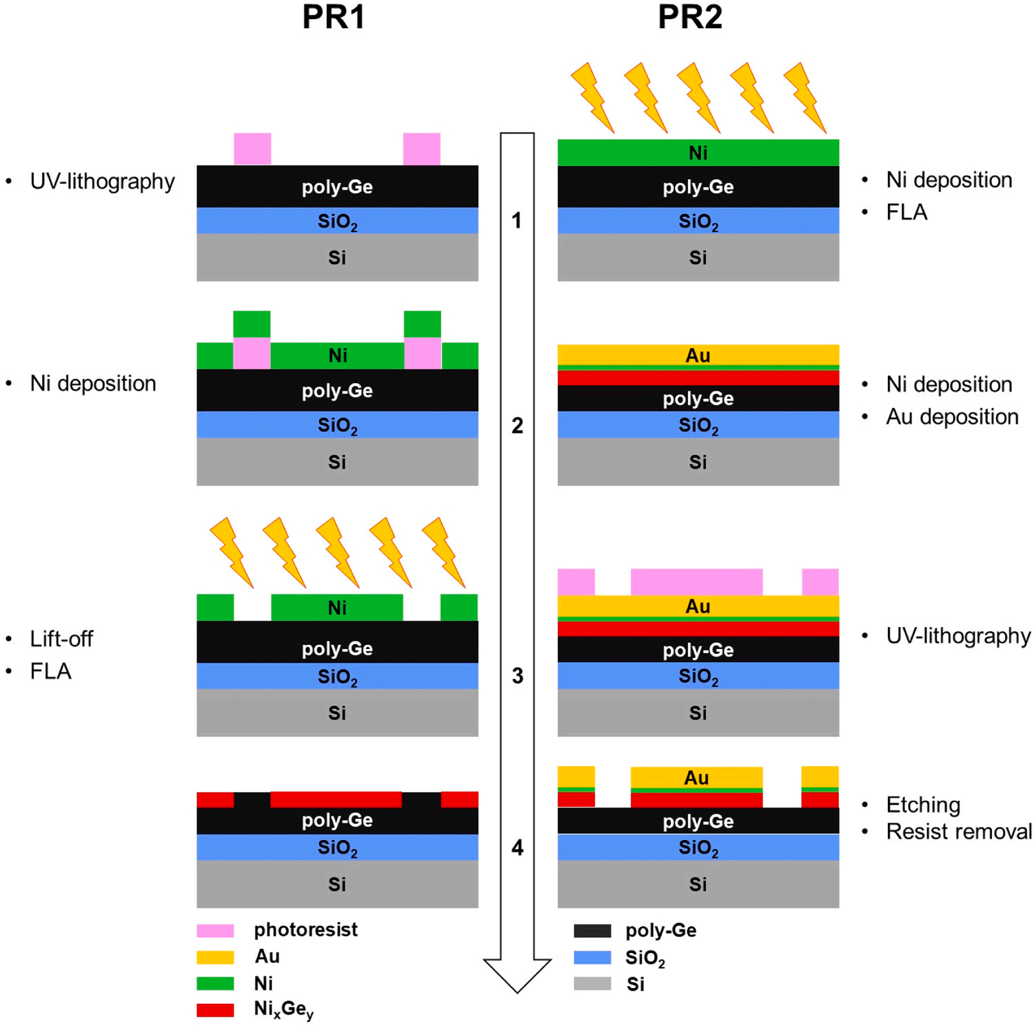
Two different process flows PR1 and PR2 were used to fabricate contacts for the cTLM, as displayed in Fig. 1a. Thereby, PR2 is an improved version of PR1 that avoid some of the shortcomings of PR1, but requires more effort in processing and has its own challenges. In the case of PR1, the poly-Ge films were dipped in CH3COOH:H2O = 1:7 to remove the native oxide from the surface. Subsequent contact patterning was performed by ma-N 1400 negative photoresist coating, UVlithography with a Süss MicroTec MA6 mask aligner, and mask developing in ma-D 533/S (step 1 in Fig. 1). In step 2, 30 nm Ni were sputtered onto the samples followed by the metal lift-off in acetone for 10 min and ethanol for 5 min in an ultrasonic bath. Finally, FLA with a 3-ms pulse was applied to the patterned sample in N2-rich atmosphere (step 3), whereby the energy density was varied in the range of 26–68 J cm− 2 . As a result, a NiGe contact embedded in the poly-Ge layer has formed (step 4).

Fig. 1. Simplified fabrication process flow PR1 and PR2.
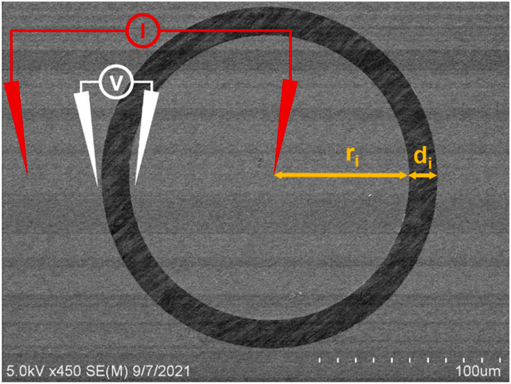
The cTLM measurements were performed on a Süss Microtec probe station in the four-probe configuration (see Fig. 2). In contrast to the linear transfer line method, there is no need to isolate the whole contact pattern by an additional mesa etch. V-I curves were measured with an injection current ranging from − 50 to 50 mA on a set of contacts with a nominal inner electrode radius (ri) of 80 μm and an electrode spacing (di) of 7–40 μm. As there is little difference between individual cTLM structures, the determination of ρc as shown in Fig. 4a is based on one cTLM structure. In the case of PR2, an additional set of contacts with ri of 50 μm and di of 3–30 μm was used as a comparative measurement. The electrode spacing was checked by optical microscopy and by scanning electron microscopy (SEM) for selected samples. Curve fitting of the V-I data was performed by a Python script with the lmfit package. X-ray diffraction patterns were recorded from plain structures by a Bruker D8 Advance Diffractometer (Karlsruhe, Germany), in asymmetric parallel beam geometry at a shallow glancing angle of 0.7◦ (Grazing Incidence Diffraction) using the Cu-Kα wavelength λ = 1.5418 Å.

Fig. 2. Top-down SEM image of a cTLM electrode with the inner electrode radius ri and the electrode spacing di. The four-point-probe measurement setup is denoted by the red (current probes) and white (voltage sensing probes) arrows.
In the case of PR1, the ρc(θpeak) is in the order of 10− 6 Ω cm2 and exhibits no or little change up to 460℃. In parallel, few percent of Nirich phases, such as Ni3Ge2, Ni3Ge, or Ni2.74Ge2, appear (Fig. 3b), which reportedly are phases of high resistivity. The second stage of the aforementioned Ni-Ge phase formation model between 460 and 540 ℃ is characterized by an initial increase of ρc, followed by a sharp decrease to the range of ca. 10− 7 Ω cm2 . This corresponds to the transition region in which Ni will be fully consumed and Ni-rich phases will decompose to NiGe and Ni, whereby the latter continues to diffuse to form NiGe in greater depth (Fig. 3b). The last stage above 600 ◦C features a region in which ρc becomes minimal with values around 2•10− 7 Ω cm2 . It can be correlated with the full transition of Ni into the stoichiometric NiGe phase (Fig. 3b).

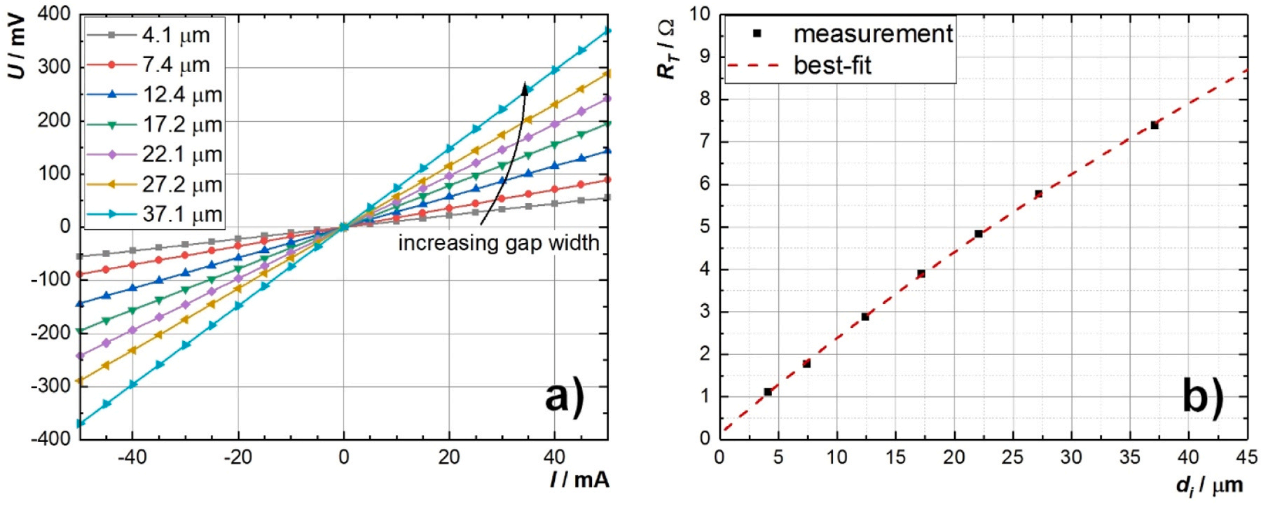
Fig. 3. (a) V-I characteristics of cTLM contacts on a sample fabricated by the PR2 process at θpeak = 600 ℃, with respect to the actual electrode gap width. In (b), the extracted total resistance (RT) is plotted against the electrode spacing and fitted.
4. Conclusion
We demonstrated that FLA as a thermal treatment with a low thermal budget is able to form NiGe on Ge with a specific contact resistivity below 10− 7 Ω cm2 , which is similar to that achieved by other thermal treatments. Based on XRD measurements, the Ni-Ge contact formation runs through stage 1 of Ni indiffusion with the first formation of Ni-rich Ni-Ge phases, stage 2 of NiGe formation in which Ni is gradually consumed to form NiGe, and the final stage 3 where NiGe is completely formed without any significant contributions from other phases.
To measure contact resistance, Ni-Ge cTLM structures were successfully fabricated on thin poly-Ge films by using two different process lines whose different advantages and weaknesses were discussed und compared to each other. In the case of the PR1 process, the contact is patterned first by a lift-off process followed by FLA, which delivered an average value of (2.2 ± 0.5) × 10− 7 Ω cm2 for the contact resistance for samples annealed beyond 570 ◦C. However, this value is biased because of the non-zero resistance of the metal itself, the difference between the Ge thicknesses below the contact and in the gap, the additional current paths between electrode sidewalls, the uncertainty of di, and the unfavorable effects of the lift-off process.